Multilayer ceramic electronic component

a technology of electronic components and ceramics, applied in the direction of fixed capacitor details, stacked capacitors, fixed capacitors, etc., can solve the problems of reducing the lifetime of high temperature accelerated devices, reducing the capacitance obtained, and unable to obtain desired properties, etc., to achieve the effect of enhancing the effect, reducing the properties of the dielectric layer (existing between the electrode layers), and enhancing the

Active Publication Date: 2012-02-02
TDK CORPARATION
View PDF1 Cites 14 Cited by
  • Summary
  • Abstract
  • Description
  • Claims
  • Application Information

AI Technical Summary

Benefits of technology

[0008]The present invention has been made in view of the above conditions, and its purpose is to provide a multilayer ceramic electronic component, showing increase in the obtained capacitance due to favorable specific permittivity, low dielectric loss and excellent high temperature accelerated lifetime, even when a dielectric layer is made further thinner.
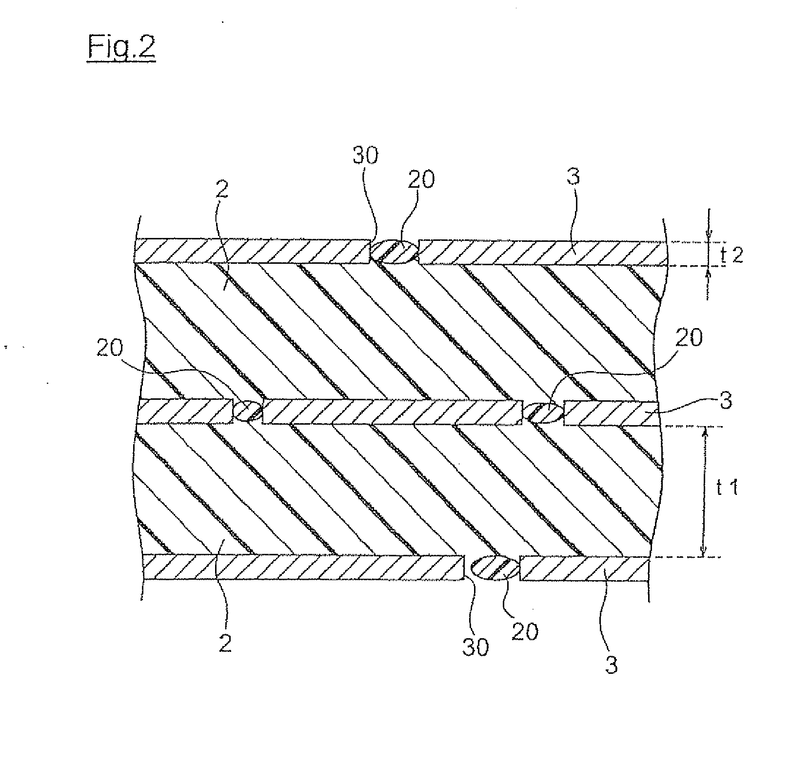
[0011]In the present invention, the segregation phase containing Mg is formed in the electrode missing portion. Also, although the segregation phase may be formed between the electrode layers (i.e. in the dielectric layer) unless deteriorating properties of the dielectric layer (e.g. specific permittivity, etc.), it is preferred not to be formed between the electrode layers. While Mg suppresses grain growth of dielectric particles, the properties of the dielectric layer may be lowered when Mg is present in the dielectric layer sandwiched between the electrode layers. However, it is possible to suppress grain growth of the dielectric particles without disturbing the properties of the dielectric layer (existing between electrode layers) by controlling a position where the segregation phase containing Mg exists.
[0013]When the coverage is within the above range, the segregation phase can securely be formed in the electrode missing portion not between the electrode layers, resulting in maximizing the above effect. In particular, by making the thicknesses of the dielectric layer and electrode layer within the above range, the coverage can easily be made within the above range.
[0016]In the multilayer ceramic electronic component according to the present invention, the segregation phase containing Mg is formed in the electrode missing portion of the electrode layer. Therefore, even with the presence of such a segregation phase, properties of the dielectric layer (existing between the electrode layers) may not be lowered. Consequently, even when the dielectric layer is made thinner, it is possible to obtain a multilayer ceramic electronic component having high reliability and favorable properties.

Problems solved by technology

However, for making the dielectric layer thinner, when a grain size of a dielectric particle is decreased specific permittivity is declined, so that desired properties may not be obtained.
However, there are problems such that the obtained capacitance may be declined because of the existence of a discontinuous portion in the internal electrode, and that high temperature accelerated lifetime may be lowered in the region where the thickness of the ceramic layer is several microns or less.
Also, Japanese Unexamined Patent Publication No H10-12476 fails to disclose specific contents of components included in the dielectric ceramic layer.

Method used


Image

  • Multilayer ceramic electronic component
  • Multilayer ceramic electronic component
  • Multilayer ceramic electronic component

Examples


example 1

[0086]Firstly, BaTiO3 powder having BET specific surface area of 8.0 m2 / g as a raw material of the main component, and MgCO3, Y2O3 and SiO2 as raw materials of the subcomponents were respectively prepared.

[0087]Secondly, the above prepared BaTiO3 powder and raw materials of the subcomponents were wet pulverized by a ball mill for 15 hours, and dried to obtain the dielectric raw material. Note that an additive amount of each subcomponent was set such that the contents of the subcomponents in the dielectric layer after firing per 100 moles of BaTiO3 as the main component were equal to the amounts shown in Table 1. Also, MgCO3 was included as MgO in the dielectric ceramic composition after firing.

[0088]Then, 100 parts by weight of the obtained dielectric raw material, 10 parts by weight of polyvinyl butyral resin, 5 parts by weight of dioctyl phthalate (DOP) as a plasticizer, and 100 parts by weight of alcohol as a solvent were mixed by a ball mill to form a paste, so that the dielectr...

example 2

[0115]Except for the content of the oxide of Mn to the value in Table 2, the multilayer ceramic capacitor sample was prepared as with sample No. 1, and property evaluation was done as in Example 1. The results are shown in Table 2.

TABLE 2segregationsampleMnOphase containingspecificNo[mol]Mnpermittivity ε310.05none345010.15none3360320.3none3150330.5none2680340.8found2450351.0found2200

[0116]From Table 2, it was confirmed that when the content of the oxide of Mn was within the preferable range of the present invention, no segregation phase containing Mn was formed, and favorable specific permittivity was obtained. On the other hand, it was confirmed that when the content of the oxide of Mn was out of the preferable range of the present invention, the specific permittivity was reduced and that the segregation phase containing Mn tended to be formed.


PUM

PropertyMeasurementUnit
thicknessaaaaaaaaaa
BET specific surface areaaaaaaaaaaa
particle diameteraaaaaaaaaa

Abstract

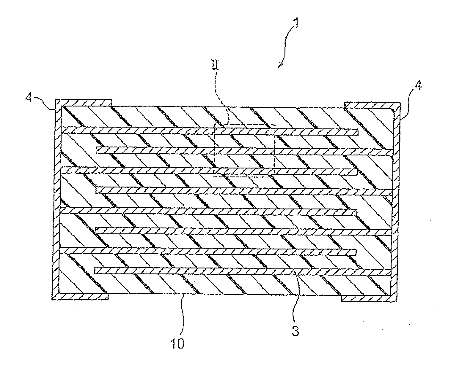
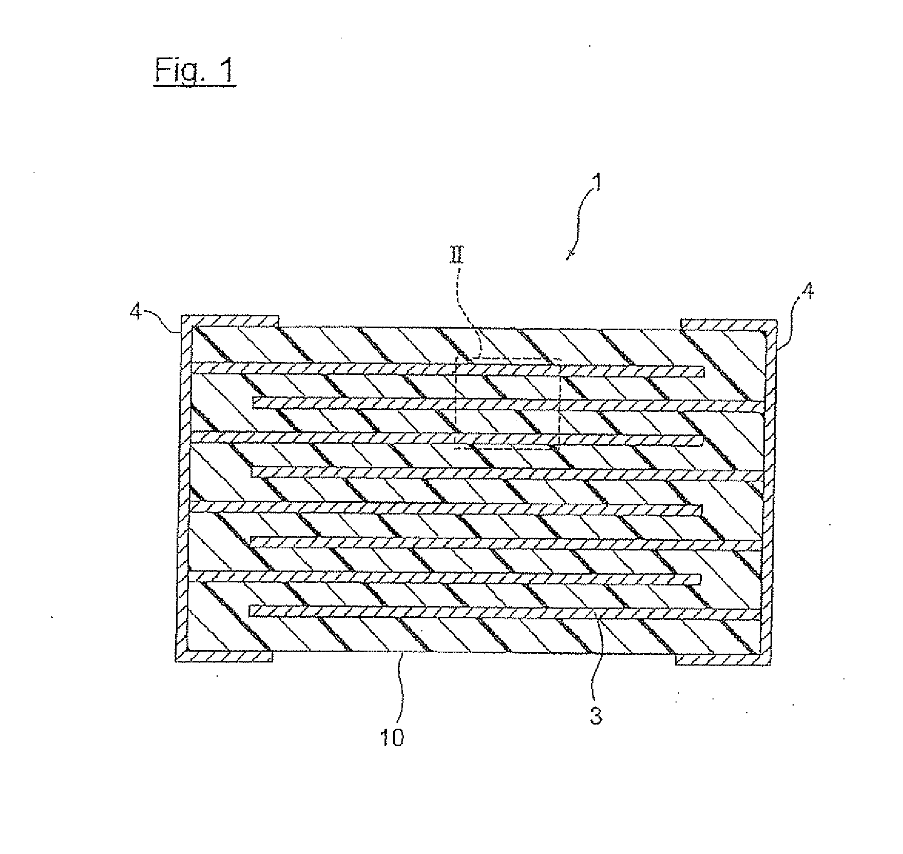
Disclosed is a multilayer ceramic electronic component, comprising an element body obtained by stacking dielectric layers (thickness t1) and electrode layers (thickness t2). The dielectric layer (2) includes a compound expressed by ABO3 (A includes Ba, and may include Ca or Sr; and B includes Ti, and may include Zr or Hf), and includes 0.75 to 2.0 moles of MgO, 0.4 to 1.0 mole of an oxide of Y, Dy, Ho and the like in terms of the oxide, and 0.4 to 0.8 mole of SiO2 per 100 moles of the compound. A segregation phase (20) containing Mg is formed in at least a part of an electrode missing portion (30), where the electrode layer is supposed to be formed but no electrode layer is formed. Line coverage of the electrode layer (3) is 60 to 90% and relations of 0.3≦t1≦2.0 and 0.3≦t2<1.0 are fulfilled.

Description

BACKGROUND OF THE INVENTION[0001]1. Field of the Invention[0002]The present invention relates to a multilayer ceramic electronic component; and a multilayer ceramic electronic component showing favorable dielectric properties even when a dielectric layer is made thinner.[0003]2. Description of the Related Art[0004]A multilayer ceramic capacitor as one example of multilayer ceramic electronic components is widely used as a small-sized, high performance, highly-reliable electronic component, and there are a large number of multilayer ceramic capacitors used in electric and electronic equipments. Recently, with downsizing and increase in performance of equipments, demands for further downsizing, higher performance and higher reliability to the multilayer ceramic electronic component have been increased.[0005]To respond the above demands, for example, a dielectric layer of the multilayer ceramic capacitor has been made thinner and increased in number of layers. However, for making the d...

Claims


Application Information

Patent Timeline
Patent Type & Authority Applications(United States)
IPC IPC(8): H01G4/12
CPCC04B35/4682H01G4/30C04B2235/3224C04B2235/3225C04B2235/3262C04B2235/3418C04B2235/5409C04B2235/6025C04B2235/6582C04B2235/6584C04B2235/663C04B2235/80C04B2235/81H01G4/1227C04B2235/3206
Inventor KANEKO, TOSHIHIKOYAMAZAKI, RYUTAROMASUKO, TAISUKESATO, YUSUKEMATSUYAMA, YASUSHIWATANABE, YASUOHOSONO, MASAKAZUTAKEDA, SAORITANAKA, HIROBUMIENDO, MAKOTO
Owner TDK CORPARATION
Why Eureka
Try Eureka