Graphene transistor with a self-aligned gate

a graphene transistor and gate technology, applied in the field of graphene devices, can solve the problems of limiting the performance of the graphene transistor, adversely affecting the device behavior, and limiting the performance of the devi

Active Publication Date: 2012-03-08
GLOBALFOUNDRIES US INC
View PDF4 Cites 68 Cited by
  • Summary
  • Abstract
  • Description
  • Claims
  • Application Information

AI Technical Summary

Benefits of technology

[0006]The gate electrode is aligned to the source and drain electrodes without the constraints inherent in lithographic alignment procedures. Thus, the lateral spacing between the sidewalls of the first electrode and the source / drain electrodes can be a sublithographic dimension. The bilayer metal gate stack, in which the second metal portion overhangs the first metal portion, is employed in this disclosure to produce geometry including an undercut in the gate stack, thereby enabling the lateral isolation between the gate electrode and the source / drain electrodes.

Problems solved by technology

One of the critical factors currently limiting the performance of graphene FETs is the parasitic series resistance between the source / drain contacts and the gated graphene channel.
However, the access regions inevitably increase the resistance of the graphene FET, thereby reducing the current through the graphene FETs and limiting the device performance.
Reduction of the access resistance is especially crucial to scale down graphene devices because the access resistance can become comparable to the resistance of the gated channel and adversely affect the device behavior significantly as the device dimensions shrink.
In the case of a graphene transistor, however, ion implantation cannot be employed because implanted dopant ions readily and inevitably destroy the fragile lattice structure of the graphene layer.

Method used


Image

  • Graphene transistor with a self-aligned gate
  • Graphene transistor with a self-aligned gate
  • Graphene transistor with a self-aligned gate

Examples


Embodiment Construction

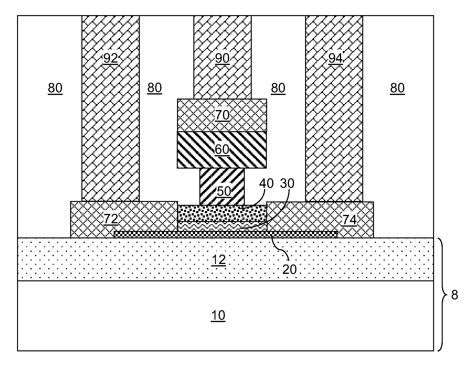
[0024]As stated above, the present disclosure relates to a graphene transistor having a self-aligned gate and methods of manufacturing the same, which are now described in detail with accompanying figures. It is noted that like reference numerals refer to like elements across different embodiments.

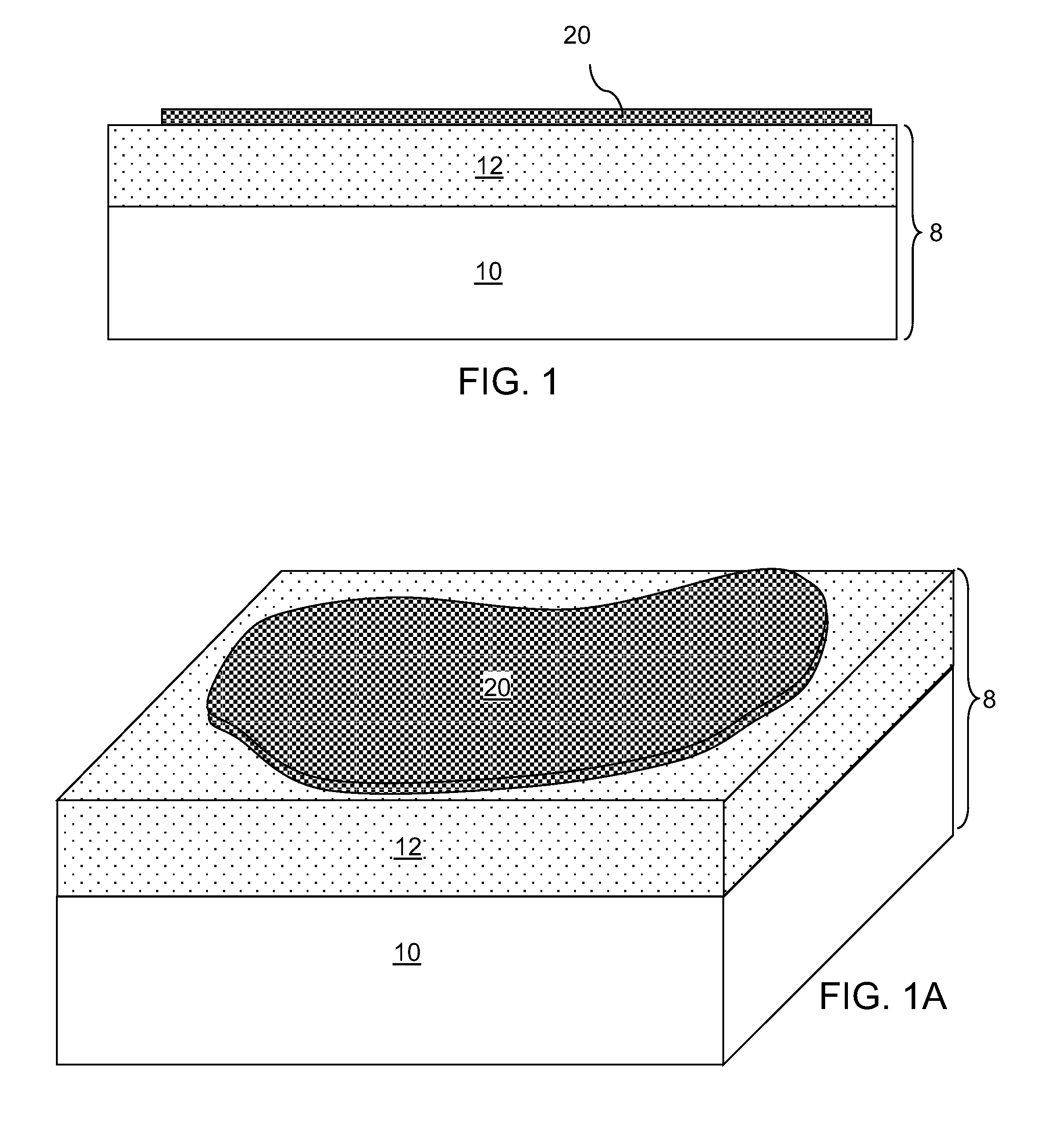
[0025]Referring to FIGS. 1 and 1A, an exemplary structure according to the present disclosure includes a graphene layer 20 formed on a substrate 8. The substrate 8 includes an insulating layer 12 located at a top portion thereof. The insulating layer 12 includes a dielectric material that does not conduct electricity. For example, the insulating layer 12 may include silicon oxide, silicon nitride, a dielectric metal oxide such as aluminum oxide, a dielectric metal nitride, or a combination thereof. Optionally, the substrate 8 may additionally include at least substrate layer 10, which may be a semiconductor layer, a conductive layer, or another insulating layer.

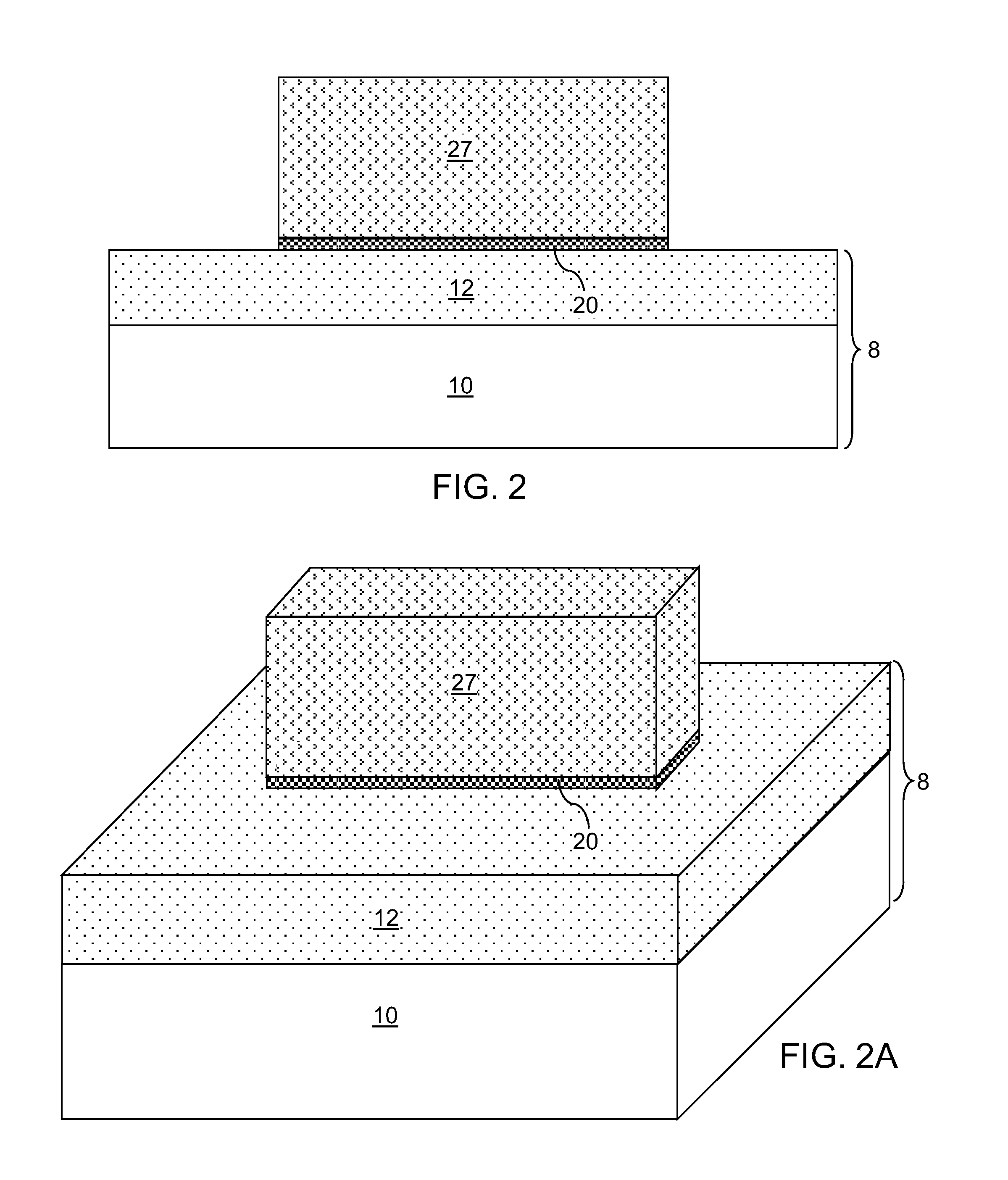
[0026]A graphene layer 20 is...


PUM

PropertyMeasurementUnit
dielectric constantaaaaaaaaaa
cut-off frequenciesaaaaaaaaaa
thicknessaaaaaaaaaa

Abstract

A graphene-based field effect transistor includes source and drain electrodes that are self-aligned to a gate electrode. A stack of a seed layer and a dielectric metal oxide layer is deposited over a patterned graphene layer. A conductive material stack of a first metal portion and a second metal portion is formed above the dielectric metal oxide layer. The first metal portion is laterally etched employing the second metal portion, and exposed portions of the dielectric metal oxide layer are removed to form a gate structure in which the second metal portion overhangs the first metal portion. The seed layer is removed and the overhang is employed to shadow proximal regions around the gate structure during a directional deposition process to form source and drain electrodes that are self-aligned and minimally laterally spaced from edges of the gate electrode.

Description

BACKGROUND[0001]The present disclosure relates to a graphene device, and particularly to a graphene transistor having a self-aligned gate and methods of manufacturing the same.[0002]The high mobility of charge carriers in graphene combined with the ability to modulate the carrier concentration by an external electric field has made graphene-based field effect transistors (FETs), or “graphene FETs,” promising candidates for future high frequency applications. Recently, graphene FETs have been demonstrated to operate at cut-off frequencies (fT) as high as 100 GHz. Additional increases in fT may be achievable through further improvement of both the constituent device materials and the device design. One of the critical factors currently limiting the performance of graphene FETs is the parasitic series resistance between the source / drain contacts and the gated graphene channel.[0003]Graphene FETs include access regions in a graphene layer, which are between a gate and source / drain elect...

Claims


Application Information

Patent Timeline
Patent Type & Authority Applications(United States)
IPC IPC(8): H01L29/76H01L21/335
CPCH01L29/1606H01L29/41733H01L29/42384H01L29/778H01L29/66742H01L29/78684H01L29/4908H01L29/7781
Inventor AVOURIS, PHAEDONFARMER, DAMON B.LIN, YU-MINGZHU, YU
Owner GLOBALFOUNDRIES US INC
Why Eureka
Try Eureka