
Light-emitting diode package

Inactive Publication Date: 2012-03-15
KIM KANG
View PDF26 Cites 34 Cited by
  • Summary
  • Abstract
  • Description
  • Claims
  • Application Information

AI Technical Summary

Benefits of technology

[0016]It is, therefore, an object of the present invention to provide an LED package capable of implementing a heat dissipation structure for enhancing LED efficiency and lengthening a life span at a low cost. Also, another object of the present invention is to provide a method for increasing the heat releasing efficiency of the LED package by improving a bonding method between the LED package and a metal plate (or a heat sink).

Problems solved by technology

The efficiency and life span of the LED are impaired as hotter heat is generated from a bonded surface of the LED.
An increase in the temperature of the LED chip increases a failure rate of the LED package.
As for a resin molding type LED package, low thermal conductivity of plastic resin hinders the provision of an efficient heat dissipation structure (or a heat sinking structure) in an LED chip of at least 0.2 W / mK.
However, such a resin molding type LED package may experience cracking between a resin material and a metal core for a heat sink due to their different thermal expansion coefficients, thus causing a reliability issue.
This structure has excellent heat dissipation properties but may create a reliability issue, such as the oxidation of an electrode or the like which results from the infiltration of moisture or air since the difference in thermal expansion coefficient with transparent silicon or resin filled in a portion that emits light causes a gold wire for connection with an electrode surface of the LED chip to be cut or the interface between metal and silicon or resin is cracked.
The alumina having a thermal conductivity of between 15 W / mK and 20 W / mK, which is lower than that of metal, is suitable for an LED package of 0.2-watt to 1-watt grade, and the LTCC having a low thermal conductivity of 3 W / mK is inadequate for a high-power LED package.
However, this LED package requires the selection of a high-priced special material in order to sinter heterogeneous ceramics and metal at the same time, and highly complicated process management is required, thus resulting in significantly high manufacturing costs.
In this case, however, the thermal grease has thermal conductivity as low as about 2 to 3 W / mK, hindering a heat flow.

Method used


Image

  • Light-emitting diode package
  • Light-emitting diode package
  • Light-emitting diode package

Examples


first embodiment

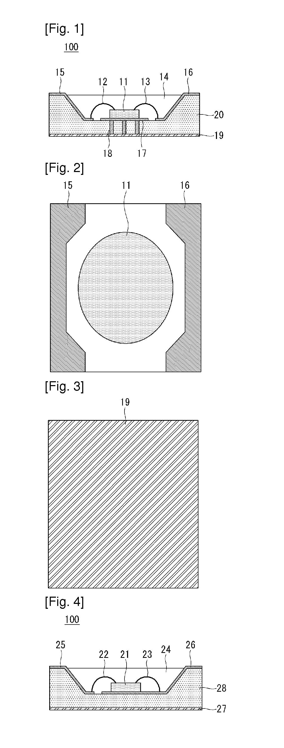
[0048]With reference to FIG. 1, an LED package 100 according to the present invention includes a package body 20, an LED chip 11, gold wirings 12 and 13, an anode electrode 15, a cathode electrode 16, a resin layer 14, a top heat transfer metal layer 17, a bottom heat transfer metal layer 19, and a heat transfer metal filler 18.

[0049]The package body 20 may be made of a resin or a ceramic material. A recess is formed on an upper surface of the package body 20. The top heat transfer metal layer 17 is formed on the bottom of the recess, and the LED chip 11 is soldered on the top heat transfer metal layer 17. The top heat transfer metal layer 17 is formed between the anode electrode 15 and the cathode electrode 16, and spaced apart from the electrodes 15 and 16. An inner side wall of the package body 20 defining the recess includes sloped faces to enhance light reflection efficiency. The anode and cathode electrodes 15 and 16 are formed on the sloped faces, namely, on the upper portion...

second embodiment

[0053]FIG. 4 is a sectional view of an LED package according to the present invention.

[0054]With reference to FIG. 4, the LED package 100 according to the second embodiment of the present invention includes a package body 28, an LED chip 21, gold wirings 32 and 33, an anode electrode 25, a cathode electrode 26, a resin layer 24, and a bottom heat transfer metal layer 27. The anode electrode 25 and the cathode electrode 26 may be switched.

[0055]The package body 28 may be made of a resin or a ceramic material. A recess is formed on an upper surface of the package body 28. The anode electrode 25 and the cathode electrode 26 are formed on the bottom of the recess, and the LED chip 21 is formed on the cathode electrode 26. An inner side wall of the package body 20 defining the recess includes sloped faces to enhance light reflection efficiency. The anode electrode 25 and the cathode electrode 26 are elongated to the sloped faces and upper faces of the package body 28. The anode electrode...

third embodiment

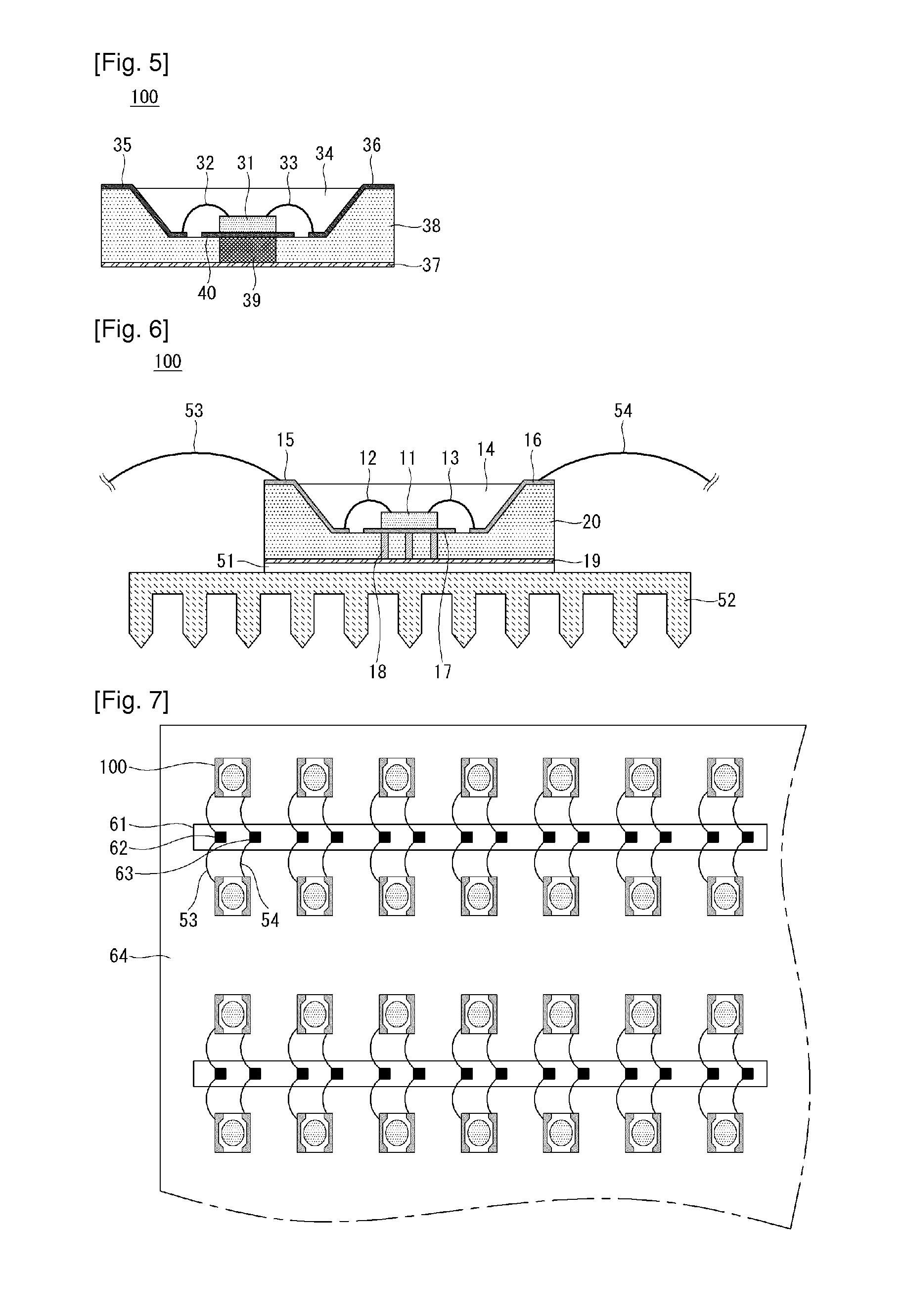
[0060]FIG. 5 is a sectional view of an LED device according to the present invention.

[0061]With reference to FIG. 5, the LED package 100 includes a package body 38, an LED chip 31, gold wirings 32 and 33, an anode electrode 35, a cathode electrode 36, a resin layer 34, a top heat transfer metal layer 40, a bottom heat transfer metal layer 37, and a heat transfer metal filler 39. The anode electrode 25 and the cathode electrode 36 may be switched.

[0062]The package body 38 may be made of a resin, or a ceramic material. A recess is formed on an upper surface of the package body 38. The anode electrode 35, the cathode electrode 36, and the top heat transfer metal layer 40 are formed on the bottom of the recess. The LED chip 31 is formed on the top heat transfer metal layer 40. The top heat transfer metal layer 40 is formed between the anode electrode 35 and the cathode electrode 36, and spaced apart from the electrodes 35 and 36 at a predetermined interval. An inner side wall of the pac...


PUM


Abstract

A light emitting diode (LED) package is provided. The LED package includes: a package body including an LED; a bottom heat transfer metal layer formed on the bottom of the package body; and a metal plate bonded to the bottom heat transfer metal layer, wherein the bottom heat transfer metal layer is bonded to the metal plate through soldering or an adhesive such as Ag epoxy, and the metal plate includes only metal without a resin layer.

Description

[0001]This application claims the benefit of Korea Patent Application No. 10-2009-0024788 filed on Mar. 24, 2009, and PCT application No. PCT / KR2010 / 001763 filed on Mar. 23, 2010, the entire contents of which are incorporated herein by reference for all purposes as if fully set forth herein.BACKGROUND OF THE INVENTION[0002]1. Field of the Invention[0003]The present invention relates to a light emitting diode package having an improved heat dissipation path by directly connecting the light emitting diode package with a metal plate.[0004]2. Related Art[0005]A light emitting diode (LED) is a two-terminal diode element including compound semiconductor materials such as GaAs, AlGaAs, GaN, InGaN, AlGaInP, or the like. The LED emits visible light with light energy generated according to recombination of electrons and holes when power is applied to a cathode terminal and an anode terminal.[0006]A white LED emitting white light may be implemented through three-color combination of a red LED,...

Claims


Application Information

Patent Timeline
IPC IPC(8): H01L27/15H01L33/64H01L33/62
CPCH01L33/486H01L33/62H01L33/641H05K1/0203H05K3/0061H05K2201/10106H01L2924/19107H01L2224/45144H01L2224/48227H01L2224/48091H01L2924/00014H01L2924/00
Inventor KIM, KANG
Owner KIM KANG
Learn More