Power amplifier
- Summary
- Abstract
- Description
- Claims
- Application Information
AI Technical Summary
Benefits of technology
Problems solved by technology
Method used
Image
Examples
first embodiment
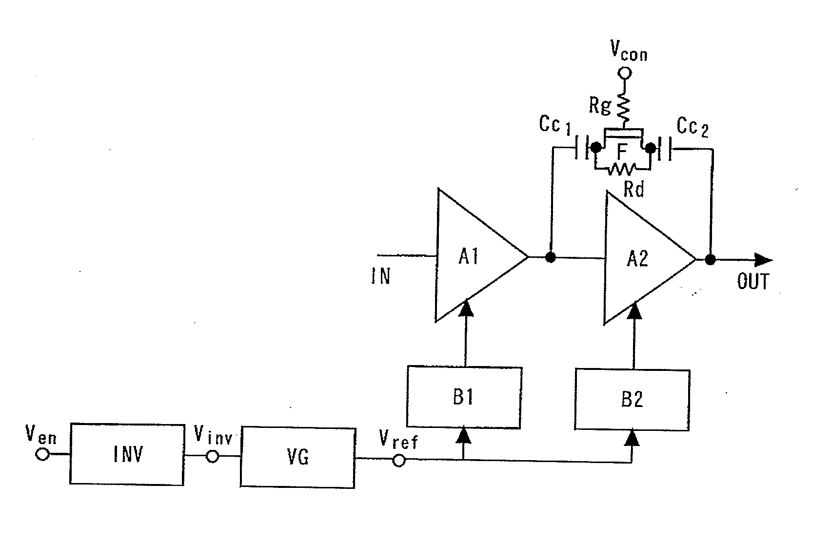
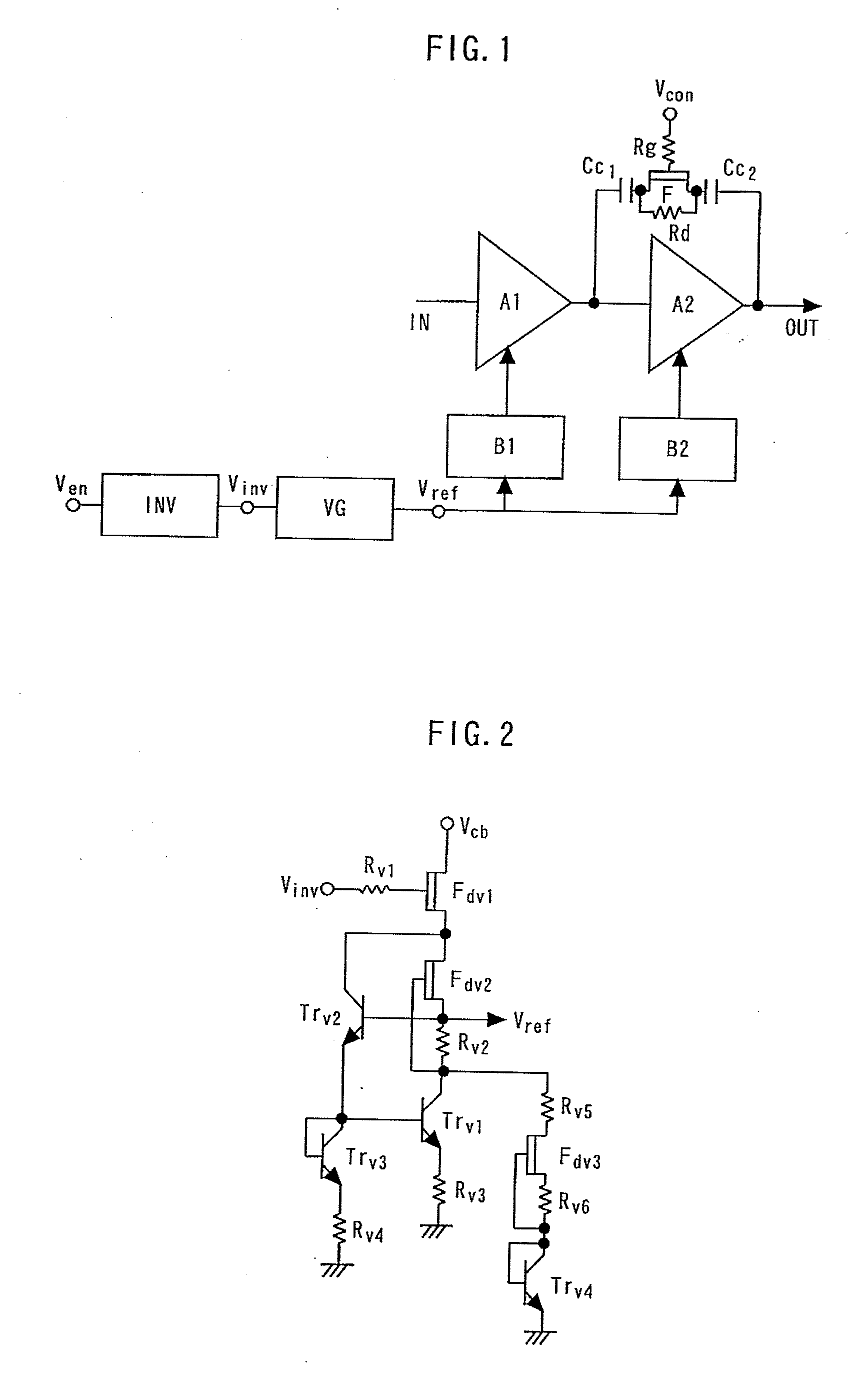
[0063]FIG. 1 is a block diagram showing a power amplifier according to the first embodiment. The power amplifier is formed using a BiFET process for fabricating a FET on the same substrate as the GaAs-HBT, and is equipped with a function for shutdown by an enable voltage inputted from the exterior.
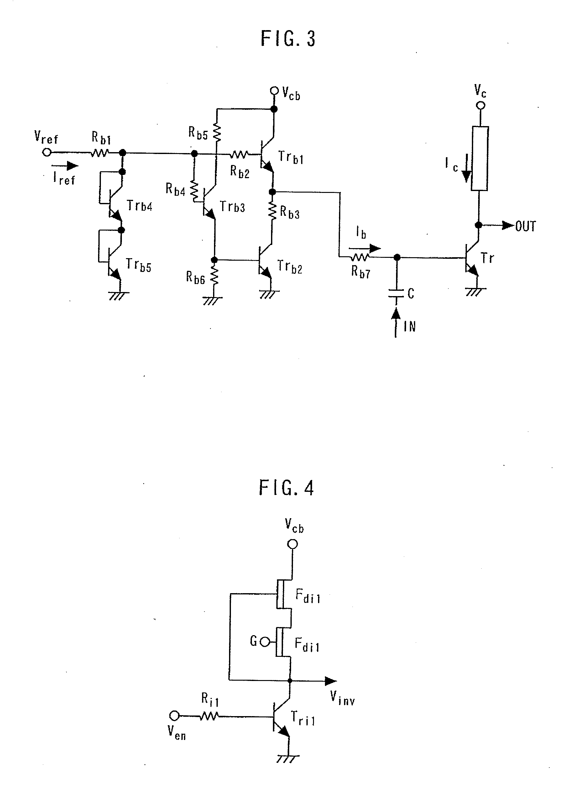
[0064]A first-stage amplifying transistor A1 and a second-stage amplifying transistor A2 for amplifying input signals are connected in series. A reference voltage generating circuit VG generates a reference voltage. A first bias circuit B1 and a second bias circuit B2 generate bias voltages on the basis of the reference voltage supplied via a terminal Vref from the reference voltage generating circuit VG, and supply bias voltages to the first-stage amplifying transistor A1 and the second-stage amplifying transistor A2, respectively.
[0065]The gate of a switch F for bypassing the second-stage amplifying transistor A2 is connected to a control terminal Vcon via a resistor Rg; the drain thereo...
second embodiment
[0076]FIG. 8 is a circuit diagram showing an inverter according to the second embodiment. In this circuit, a diode Di1 is added to the inverter in the first embodiment. The diode Di1 is connected between Fdi1 and Fdi2. The diode Di1 is a Schottky diode formed between the gate and source, and between the gate and drain of a FET, and the ON voltage thereof is about 0.6 to 0.7V. The resistance value of Fdi2 can be reduced by the ON voltage (to about ½). When the threshold voltage of the depletion mode FET is deeper than the ON voltage of the diode Di1 (for example, when the threshold voltage is −0.8 V), the circuit is effectively operated. In addition, the effect in the first embodiment can also be achieved.
third embodiment
[0077]FIG. 9 is a circuit diagram showing an inverter according to the third embodiment. In this circuit, a FET resistor Fdi3 formed by opening the gate of the depletion mode FET is added to the inverter in the second embodiment. Fdi2 and Fdi3 are connected in series.
[0078]FIG. 10 is a diagram showing the DC characteristics of two FET resistors connected in series according to the third embodiment. Since the range of linear operation is expanded to about 1.2 V, as described above, this embodiment is especially effective when the FET resistor is used in line in a wide voltage range. In addition, the effect in the second embodiment can also be achieved.
PUM
 Abstract
Description
Claims
Application Information


