Power amplifier

a power amplifier and amplifier technology, applied in the direction of gated amplifiers, high-frequency amplifiers, gain control, etc., can solve the problems of significant variation of reference voltage and collector current, negative gate bias voltage, gain variation, etc., to achieve the effect of suppressing leakage current without increasing chip area and manufacturing costs

Active Publication Date: 2012-07-10
MURATA MFG CO LTD
View PDF7 Cites 0 Cited by
  • Summary
  • Abstract
  • Description
  • Claims
  • Application Information

AI Technical Summary

Benefits of technology

[0011]Whereas in the example shown in FIG. 44, although the leakage current when the enable voltage is 0 V is good, the leakage current when the enable voltage is 0.5 V becomes larger than in the example shown in FIG. 45. Therefore, if the operation current of an inverter having no shutdown functions is 10 μA and the leakage current of other blocks is sufficiently low, the second reference example is suitable for satisfying the specifications of the enable voltage. In particular, even when the enable voltage is 0.5 V, the leakage current specification for the normally required entire power amplifier at the time of shutdown (lower than 10 μA) can be easily satisfied. However, even at the time of shutdown, the reduction of the current consumed by the continuously operating inverter is important.
[0013]In view of the above-described problems, an object of the present invention is to provide a power amplifier capable of suppressing leakage current without increasing chip areas and manufacturing costs.
[0015]The present invention makes it possible to suppress leakage current without increasing chip areas and manufacturing costs.

Problems solved by technology

Since a conventional GaAs-FET power amplifier has negative threshold voltage, it had a disadvantage that a negative gate bias voltage was required.
Such a power amplifier had a problem wherein if the threshold voltage of a depletion mode FET is varied, the reference voltage and the collector current is significantly varied.
Therefore, the depression of gain variation due to process variation is one of important issues in designing.

Method used


Image

  • Power amplifier
  • Power amplifier
  • Power amplifier

Examples


first embodiment

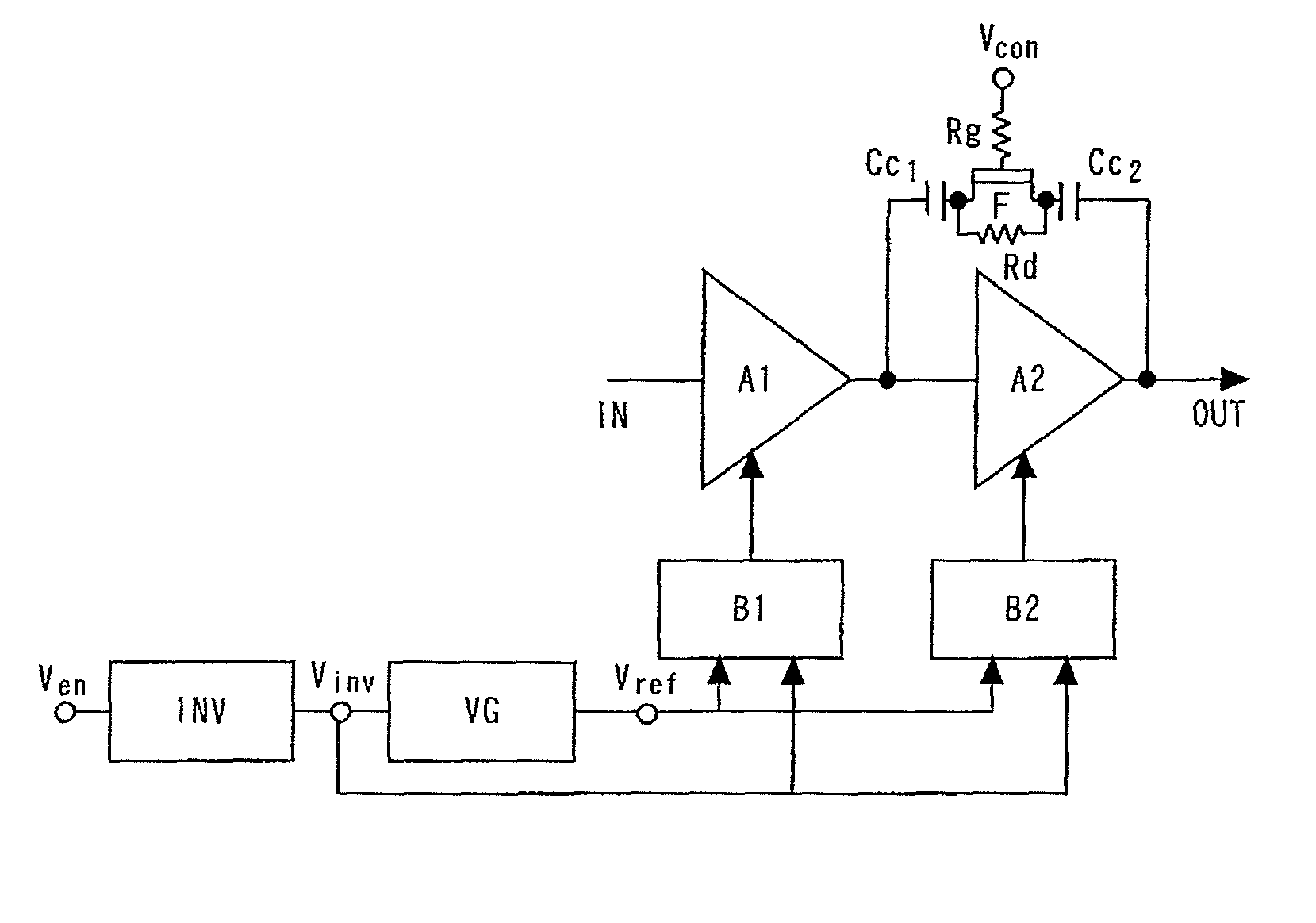
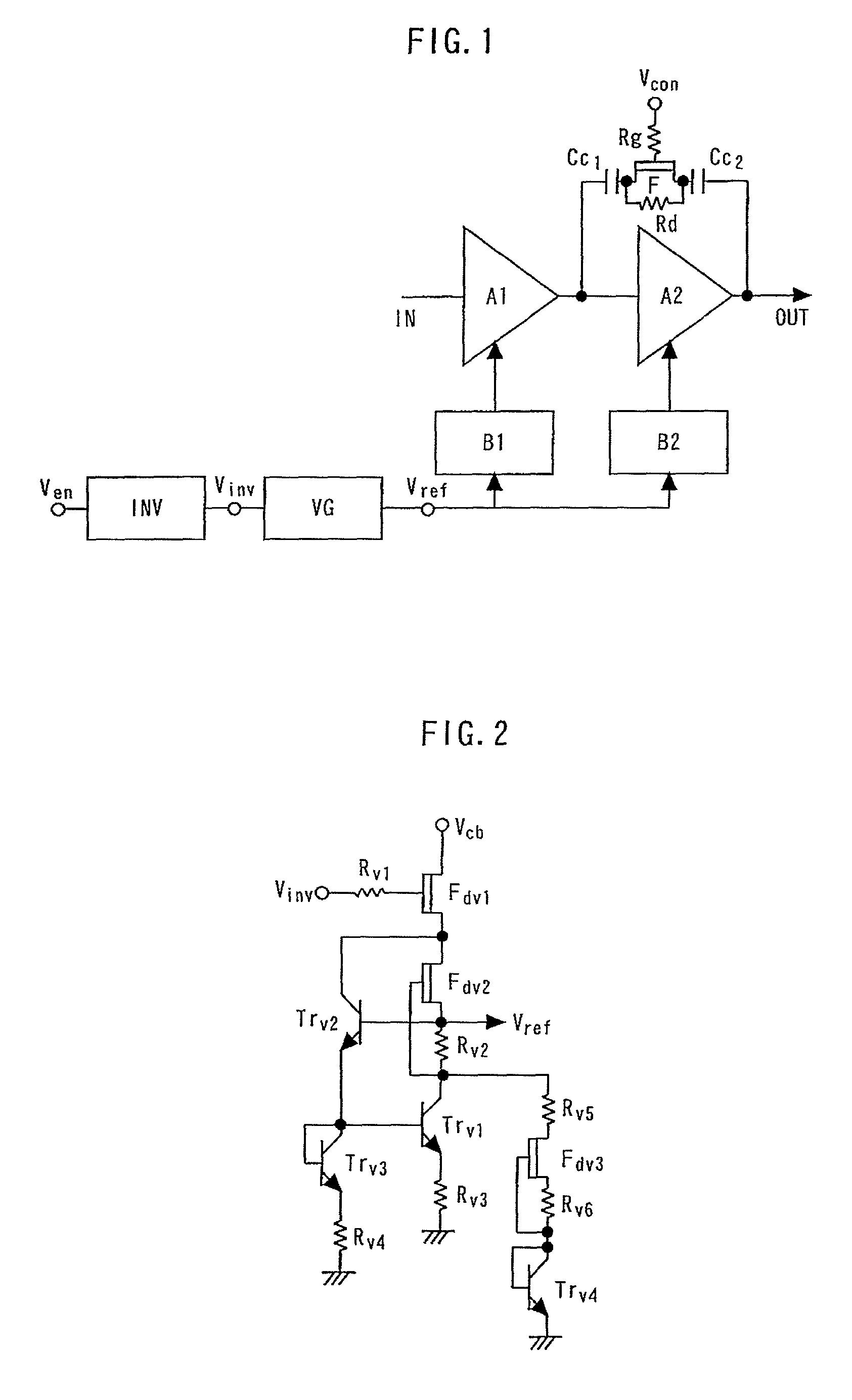
[0063]FIG. 1 is a block diagram showing a power amplifier according to the first embodiment. The power amplifier is formed using a BiFET process for fabricating a FET on the same substrate as the GaAs-HBT, and is equipped with a function for shutdown by an enable voltage inputted from the exterior.

[0064]A first-stage amplifying transistor A1 and a second-stage amplifying transistor A2 for amplifying input signals are connected in series. A reference voltage generating circuit VG generates a reference voltage. A first bias circuit B1 and a second bias circuit B2 generate bias voltages on the basis of the reference voltage supplied via a terminal Vref from the reference voltage generating circuit VG, and supply bias voltages to the first-stage amplifying transistor A1 and the second-stage amplifying transistor A2, respectively.

[0065]The gate of a switch F for bypassing the second-stage amplifying transistor A2 is connected to a control terminal Vcon via a resistor Rg; the drain thereo...

second embodiment

[0076]FIG. 8 is a circuit diagram showing an inverter according to the second embodiment. In this circuit, a diode Di1 is added to the inverter in the first embodiment. The diode Di1 is connected between Fdi1 and Fdi2. The diode Di1 is a Schottky diode formed between the gate and source, and between the gate and drain of a FET, and the ON voltage thereof is about 0.6 to 0.7V. The resistance value of Fdi2 can be reduced by the ON voltage (to about ½). When the threshold voltage of the depletion mode FET is deeper than the ON voltage of the diode Di1 (for example, when the threshold voltage is −0.8 V), the circuit is effectively operated. In addition, the effect in the first embodiment can also be achieved.

third embodiment

[0077]FIG. 9 is a circuit diagram showing an inverter according to the third embodiment. In this circuit, a FET resistor Fdi3 formed by opening the gate of the depletion mode FET is added to the inverter in the second embodiment. Fdi2 and Fdi3 are connected in series.

[0078]FIG. 10 is a diagram showing the DC characteristics of two FET resistors connected in series according to the third embodiment. Since the range of linear operation is expanded to about 1.2 V, as described above, this embodiment is especially effective when the FET resistor is used in line in a wide voltage range. In addition, the effect in the second embodiment can also be achieved.


PUM


Abstract

A power amplifier comprises: an amplifying transistor for amplifying an input signal; a reference voltage generating circuit which generates a reference voltage; a bias circuit generating a bias voltage based on the reference voltage and supplying the bias voltage to the amplifying transistor; and a booster elevating an enable voltage input from outside and outputting the enable voltage. The reference voltage generating circuit is turned ON / OFF in correspondence with an output voltage of the booster. The booster includes: an enable terminal to which the enable voltage is applied; a power source terminal connected to a power source; a transistor having a control electrode connected to the enable terminal, a first electrode connected to the power source terminal, and a second electrode that is grounded; and a FET resistor connected between the first electrode of the transistor and the power source terminal. A gate electrode of the FET resistor is open.

Description

BACKGROUND OF THE INVENTION[0001]1. Field of the Invention[0002]The present invention relates to a power amplifier formed using a BiFET process. More specifically, the present invention relates to a power amplifier capable of suppressing leakage current without increasing chip areas and manufacturing costs.[0003]2. Background Art[0004]Since a conventional GaAs-FET power amplifier has negative threshold voltage, it had a disadvantage that a negative gate bias voltage was required. On the other hand, a GaAs-HBT (hetero junction bipolar transistor) power amplifier does not require negative gate bias voltage, enables single power source operation, and has more even bias characteristics than the FET type. In recent years, therefore, a GaAs-HBT power amplifier has been actively used in mobile telephones such as CDMA or wireless LANs.[0005]Recently, a Bi-FET process for forming a FET on the same substrate for a GaAs-HBT has been increasingly applied to products. Normally, in the case of a ...

Claims


Application Information

Patent Timeline
Patent Type & Authority Patents(United States)
IPC IPC(8): H03F3/20
CPCH03F1/0277H03F3/189H03F3/195H03F3/245H03F3/72H03G1/0088H03F2200/27H03F2200/411H03F2203/7206H03F2203/7236H03F1/30H03F3/20
Inventor YAMAMOTO, KAZUYAMIYASHITA, MIYOSUZUKI, SATOSHIMATSUZUKA, TAKAYUKI
Owner MURATA MFG CO LTD
Why Eureka
Try Eureka