Reconfigurable Multi-level Sensing Scheme for Semiconductor Memories

a memory array and multi-level technology, applied in the field of semiconductor memory devices, can solve the problems of inflexibility, complex, slow, conventional sensing schemes for reading the respective states of mlcs in memory arrays, etc., and achieve the effects of simple structure, faster speed, and small chip area

Active Publication Date: 2012-03-15
GLOBALFOUNDRIES US INC
View PDF7 Cites 82 Cited by
  • Summary
  • Abstract
  • Description
  • Claims
  • Application Information

AI Technical Summary

Benefits of technology

[0006]The present invention, in illustrative embodiments thereof, relates to techniques for sensing the respective states of a MLC memory cell. Compared to conventional sensing schemes used, for example, in MLC flash memory architectures, sensing techniques according to aspects of the invention o

Problems solved by technology

However, conventional sensing schemes for reading the respective states of MLCs in a memory a

Method used


Image

  • Reconfigurable Multi-level Sensing Scheme for Semiconductor Memories
  • Reconfigurable Multi-level Sensing Scheme for Semiconductor Memories
  • Reconfigurable Multi-level Sensing Scheme for Semiconductor Memories

Examples


Embodiment Construction

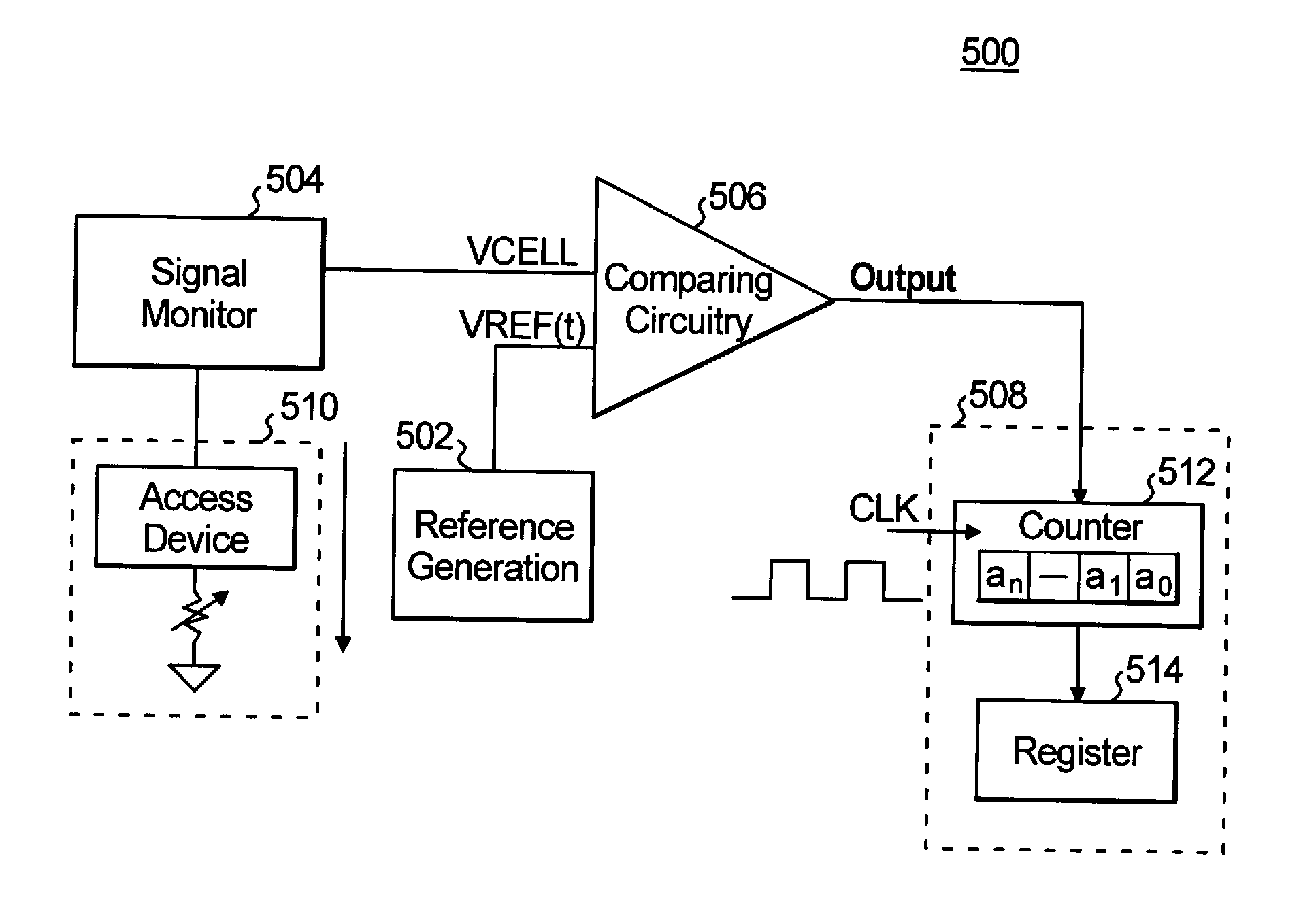
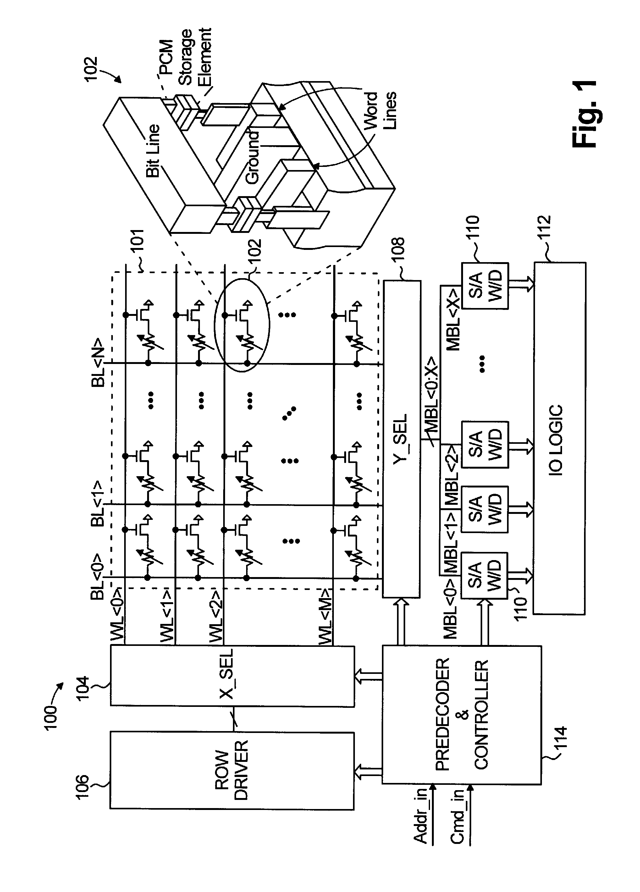
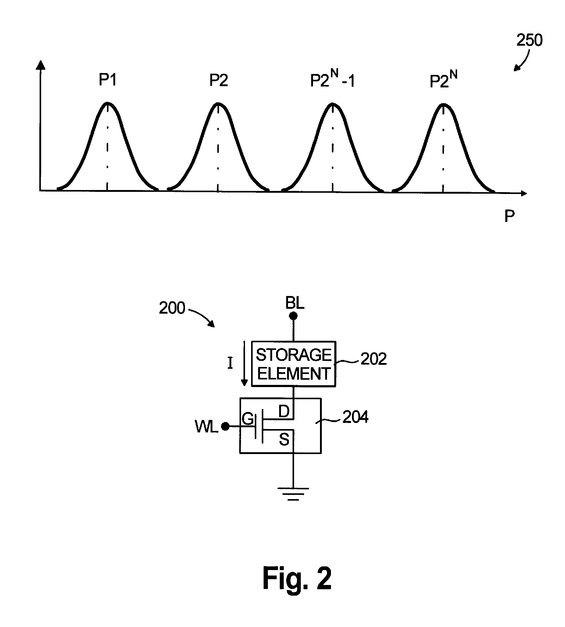
[0022]The present invention, according to embodiments thereof, will be described herein in the context of reconfigurable sensing apparatus and methods for use in a multi-level cell semiconductor memory array, particularly a multi-level cell phase change memory (PCM), whether embedded or discrete. It is to be appreciated, however, that the invention is not limited to the specific apparatus and methods illustratively shown and described herein. Rather, aspects of the invention are directed broadly to enhanced techniques for accurately sensing one or more parameters indicative of a logical state of a multi-level storage cell in a semiconductor memory. The novel sensing techniques in accordance with aspects of the invention provide, among other advantages, a simple structure which occupies a smaller chip area and enables faster sensing speeds, compared to conventional approaches. Moreover, techniques of the invention beneficially provide the flexibility to change, on the fly, a precisio...


PUM


Abstract

A method for sensing at least one parameter indicative of a logical state of a multi-level memory cell includes the steps of: measuring the parameter of the multi-level memory cell; comparing the measured parameter of the multi-level memory cell with a prescribed reference signal, the reference signal having a value which varies as a function of time; and storing a time value corresponding to a point in time at which the reference signal is substantially equal to the measured parameter of the multi-level memory cell, the stored time value being indicative of a sensed logical state of the multi-level memory cell.

Description

CROSS-REFERENCE TO RELATED APPLICATIONS[0001]This patent application claims the benefit of U.S. Provisional Patent Application Ser. No. 61 / 382,197 filed on Sep. 13, 2010, and entitled “Multi-level Sensing Scheme for Semiconductor Memories,” the disclosure of which is expressly incorporated herein by reference in its entirety for all purposes.FIELD OF THE INVENTION [0002]The present invention relates generally to semiconductor memory devices, and more particularly relates to techniques for sensing data stored in semiconductor memory devices.BACKGROUND OF THE INVENTION[0003]Typical semiconductor memories are fabricated on semiconductor substrates including arrays of a large number of physical memory cells. In general, one bit of binary data is represented as a variation of a physical parameter associated with a memory cell. Commonly used physical parameters may include, for example, threshold voltage variation of a metal-oxide-semiconductor field effect transistor (MOSFET) in a memory...

Claims


Application Information

Patent Timeline
IPC IPC(8): G11C11/00G11C7/06
CPCG11C11/5642G11C11/5678G11C13/0004G11C13/003G11C2211/5644G11C13/0061G11C23/00G11C2211/5634G11C13/004
Inventor LAM, CHUNG H.LEWIS, SCOTT C.LI, JING
Owner GLOBALFOUNDRIES US INC
Why Eureka
Try Eureka