Plasma etching apparatus, plasma etching method, and semiconductor device manufacturing method

a plasma etching and manufacturing method technology, applied in electrical devices, semiconductor devices, electric discharge tubes, etc., can solve problems such as undesirable shape, and achieve the effect of more accuracy

Active Publication Date: 2012-03-15
TOKYO ELECTRON LTD
View PDF16 Cites 228 Cited by
  • Summary
  • Abstract
  • Description
  • Claims
  • Application Information

AI Technical Summary

Benefits of technology

[0015]In accordance with the above-described plasma etching apparatus, plasma etching method and semiconductor d

Problems solved by technology

In this example, with regard to performing the etching process on the target substrate, there is a possibility that the following problems may occur.
However, by way of e

Method used


Image

  • Plasma etching apparatus, plasma etching method, and semiconductor device manufacturing method
  • Plasma etching apparatus, plasma etching method, and semiconductor device manufacturing method
  • Plasma etching apparatus, plasma etching method, and semiconductor device manufacturing method

Examples


Embodiment Construction

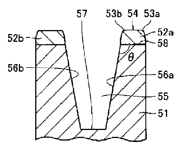
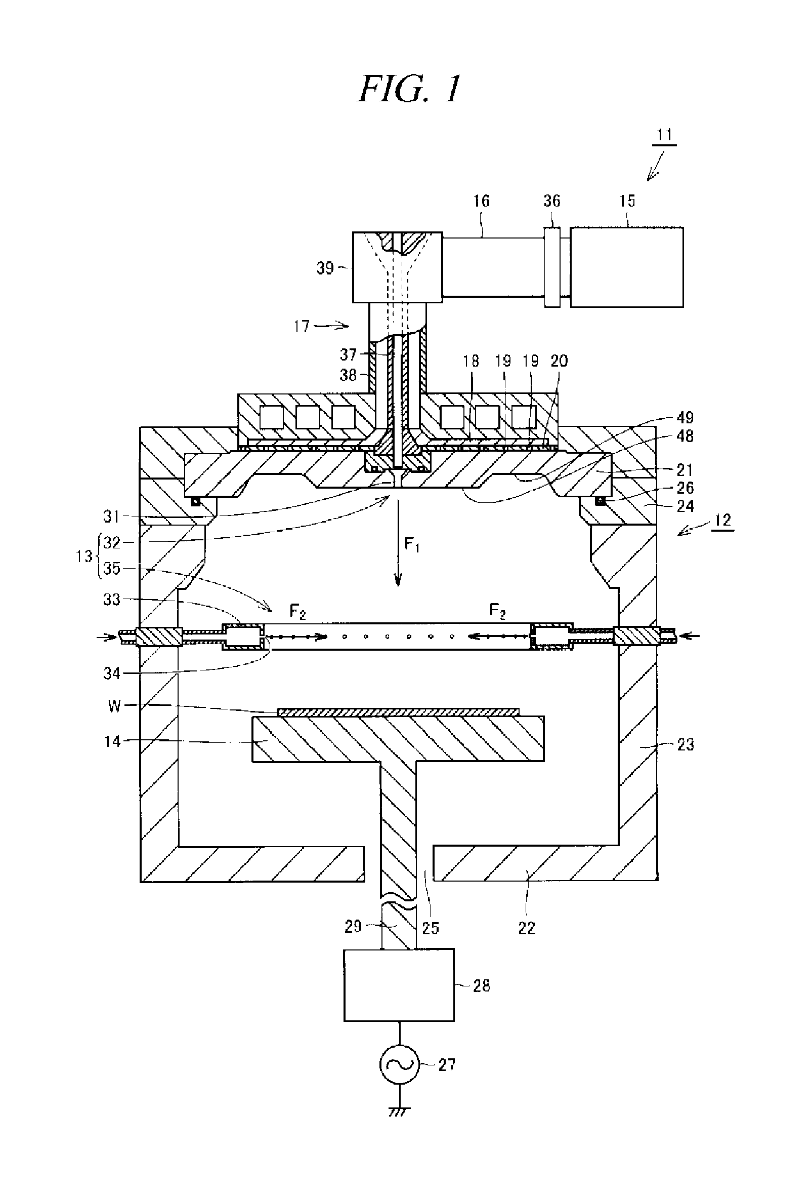
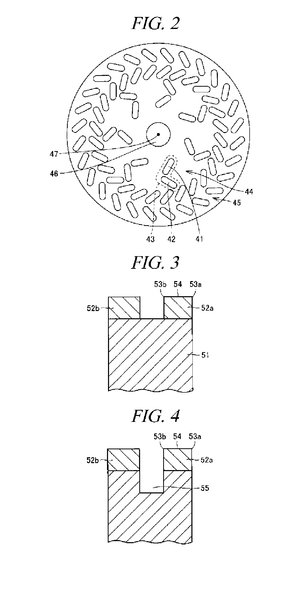
[0057]Hereinafter, embodiments of the present disclosure will be described in detail with reference to the accompanying drawings. Above all, there will be explained a configuration of a plasma etching apparatus in accordance with an embodiment of the present disclosure. FIG. 1 is a schematic cross sectional view schematically showing a configuration of a plasma etching apparatus in accordance with an embodiment of the present disclosure. FIG. 2 shows a slot antenna plate, when viewed from its thickness direction, provided in the plasma etching apparatus depicted in FIG. 1.

[0058]Referring to FIGS. 1 and 2, a plasma etching apparatus 11 may use a microwave as a plasma source. The plasma etching apparatus 11 may include a processing chamber 12 having a processing space in which a plasma process may be performed on a target substrate W; a gas supply unit 13 configured to supply a gas for a plasma process into the processing chamber 12; a supporting table 14 provided within the processin...


PUM

PropertyMeasurementUnit
Fractionaaaaaaaaaa
Fractionaaaaaaaaaa
Pressureaaaaaaaaaa

Abstract

There is provided a plasma etching apparatus provided for performing an etching in a desirable shape. The plasma etching apparatus includes a processing chamber 12 for performing a plasma process on a target substrate W; a gas supply unit 13 for supplying a plasma processing gas into the processing chamber 12; a supporting table positioned within the processing chamber 12 and configured to support the target substrate thereon; a microwave generator 15 for generating a microwave for plasma excitation; a plasma generation unit for generating plasma within the processing chamber 12 by using the generated microwave; a pressure control unit for controlling a pressure within the processing chamber 12; a bias power supply unit for supplying AC bias power to the supporting table 14; and a control unit for controlling the AC bias power by alternately repeating supply and stop of the AC bias power.

Description

CROSS-REFERENCE TO RELATED APPLICATION[0001]This application claims the benefit of Japanese Patent Application No. 2010-206536 filed on Sep. 15, 2010, the entire disclosures of which are incorporated herein by reference.FIELD OF THE INVENTION[0002]The present disclosure relates to a plasma etching apparatus, a plasma etching method, and a semiconductor device manufacturing method. In particular, the present disclosure relates to a plasma etching apparatus that performs an etching process on a target substrate, a plasma etching method using the plasma etching apparatus, and a method for manufacturing a semiconductor device by performing the etching process on the target substrate.BACKGROUND OF THE INVENTION[0003]A semiconductor device such as a LSI (Large Scale Integrated circuit) or a MOS (Metal Oxide Semiconductor) transistor is manufactured by performing a process such as etching, CVD (Chemical Vapor Deposition) or sputtering on a semiconductor substrate (wafer) serving as a targe...

Claims


Application Information

Patent Timeline
IPC IPC(8): H01L21/3065
CPCH01J37/32192H01J37/32706H01L21/3065H01L29/6656H01L21/76224H01L21/76897H01L29/6653H01L21/31116
Inventor NOZAWA, TOSHIHISASASAKI, MASARUHASHIMOTO, JUNYOSHIMURA, SHOTAOZU, TOSHIHISANISHIZUKA, TETSUYA
Owner TOKYO ELECTRON LTD
Why Eureka
Try Eureka