Different types of memory integrated in one chip by using a novel protocol

a technology of memory and chip, applied in the field of semiconductor memory, can solve the problems of getting more and more difficulty in scaling down to less than 45 nm, and achieve the effects of increasing die cost, high speed performance, and difficult circuit design

Inactive Publication Date: 2012-03-22
APLUS FLASH TECH
View PDF6 Cites 22 Cited by
  • Summary
  • Abstract
  • Description
  • Claims
  • Application Information

AI Technical Summary

Benefits of technology

[0018]10. A Write-While-Write for multiple write functions is provided to different nonvolatile memories simultaneously once the corresponding write command is issued. This operation accelerates the program performance.
[0019]11. A Read-While-Write function provides flexibility to read the memory while one or more nonvolatile memories (except the SRAM) are processing the write operation.
[0020]12. A Read-While-Transfer operation is available once the read operation is applied to SRAM, EEPROM and NOR flash and the data of a NAND cell is transferred to a page buffer (data register) during the page read operation. This operation accelerates the read performance.
[0021]13. A Write-While-Transfer operation once the write operation is applied to a SRAM, EEPROM and NOR flash and the data of the NAND cell is transferred to a page buffer (data register) during the page read operation. This operation accelerates the write performance.
[0023]The present invention relates generally to a novel unified nonvolatile memory design that preferably uses an economic process, i.e. NAND-like process to make NOR flash, NAND flash, EEPROM and SRAM, wherein the NOR flash stores code, the NAND and EEPROM store large and small amount of data, respectively, and the SRAM can be used as the cache storage for high speed performance such as in XIP (execute in place) operation. The unified nonvolatile memory design offers the flexibility in memory storage for different applications and overcoming the disadvantage of parallel interfaces that increase external pins of the die and result in increased die cost. In addition the pin number would not be a constant and additional address pins would be required when density is being doubled, which would make circuit design difficult and not forward and backward compatible with different memory density.
[0024]The novel SRAM, EEPROM, NAND and NAND-based NOR hybrid memory design with multiple interfaces and multiple input and output pins within fixed pin numbers for all densities provides a great advantage for achieving the highest memory density, and provides a unique sequence to enter into different interface protocols.

Problems solved by technology

In the past 20 years, the cell structure, program and erase schemes and manufacturing process for NAND and NOR logic circuits have been incompatible preventing both products from being integrated into one chip.
The conventional ETOX-based NOR cell has a cell size that is approximately 12-16λ2 and is getting more and more difficulty to scale down below 45 nm.

Method used


Image

  • Different types of memory integrated in one chip by using a novel protocol
  • Different types of memory integrated in one chip by using a novel protocol
  • Different types of memory integrated in one chip by using a novel protocol

Examples


Embodiment Construction

[0035]Hereinafter, the present invention will be described in detail. However, the present invention is not limited to the timing waveforms disclosed below, but can be implemented to expand more command clock cycles. The following is described in order to enable those of ordinary skill in the art to embody and practice the present invention.

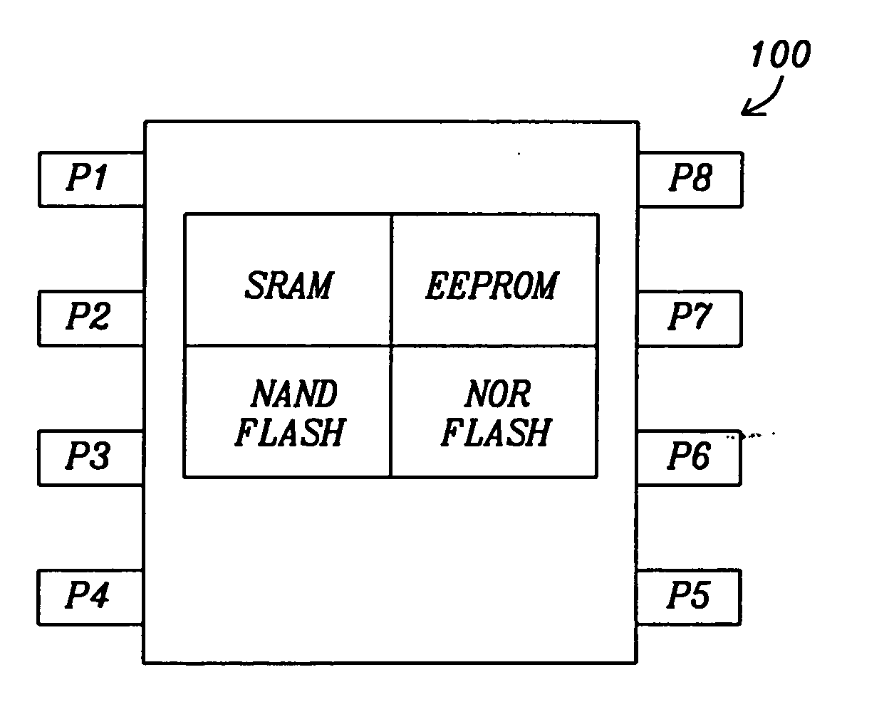
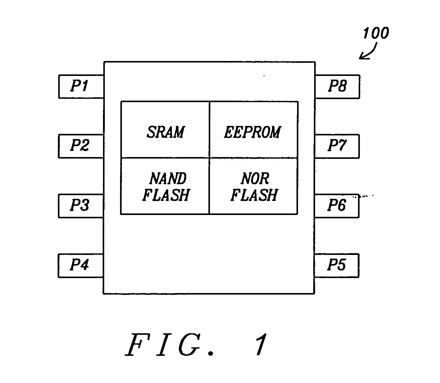
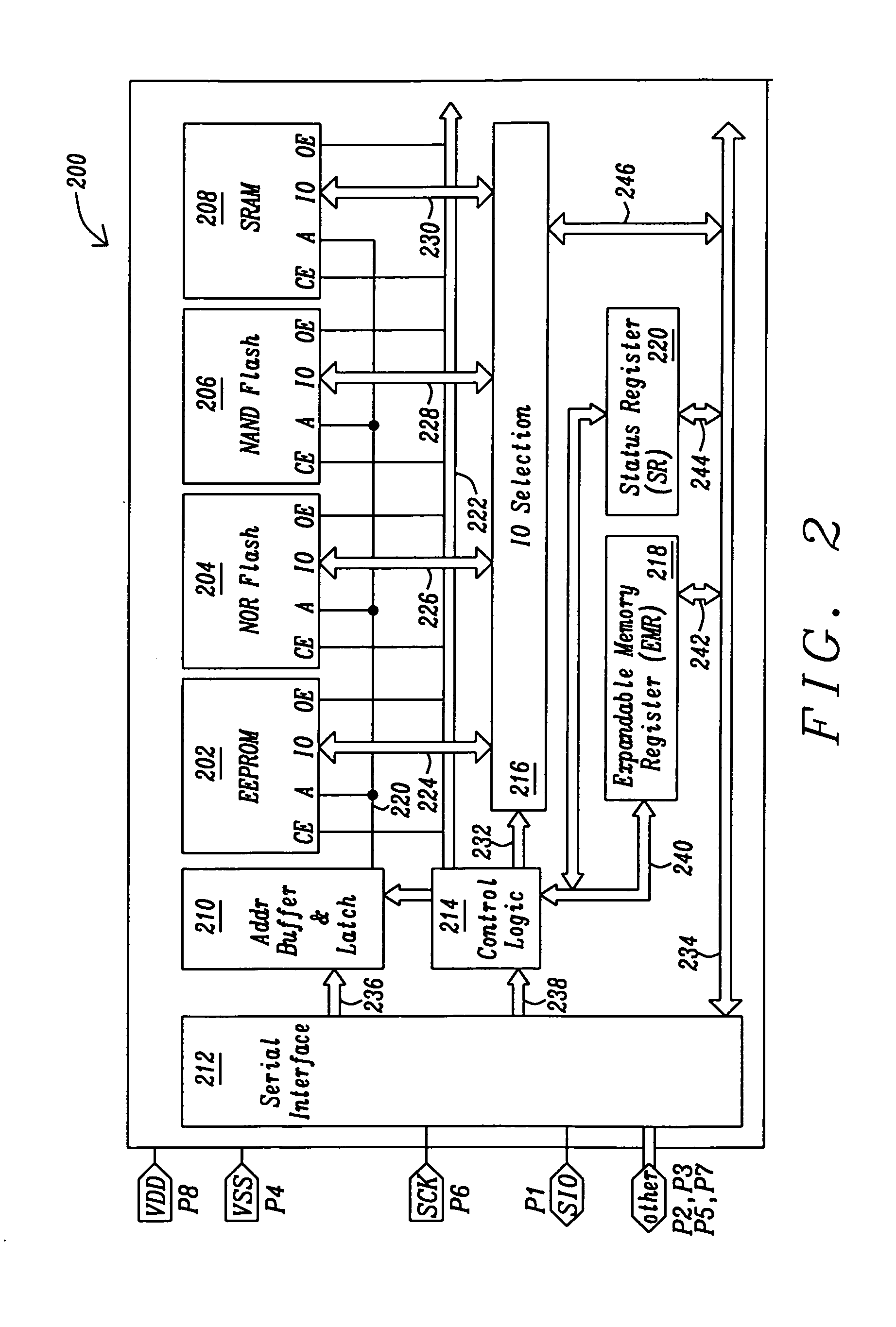
[0036]FIG. 1 is an eight-pin packaged chip 100. The package includes four types of memory, i.e. EEPROM, NOR Flash, NAND Flash and SRAM integrated into one chip and is featured for low-power, high-performance operation in a low pin-count package. System designs using eight-pin memory devices occupy less board space and ultimately lower system costs. The high performance and small footprint of the device make it an ideal choice for mobile handsets, Bluetooth® headsets, optical disk drives, GPS applications and other portable electronic products.

TABLE 1InterfaceI2CSPISDISQIPin #Pin NameP1SIOSIOSIOSIOP2NCSOSO[0]SIO[1]P3NCNCSO[1]SIO[2]P4VSSVSSVSSVSSP5...


PUM

PropertyMeasurementUnit
cell sizeaaaaaaaaaa
sizeaaaaaaaaaa
densityaaaaaaaaaa

Abstract

A semiconductor chip contains four different memory types, EEPROM, NAND Flash, NOR Flash and SRAM, and a plurality of major serial / parallel interfaces such as I2C, SPI, SDI and SQI in one memory chip. The memory chip features write-while-write and read-while-write operations as well as read-while-transfer and write-while-transfer operations. The memory chip provides for eight pins of which two are for power and up to four pins have no connection for specific interfaces and uses a novel unified nonvolatile memory design that allow the integration together of the aforementioned memory types integrated together into the same semiconductor memory chip.

Description

[0001]This application claims priority to Provisional Patent Application Ser. No. 61 / 403,556, filed on Sep. 17, 2010, which is herein incorporated by reference in its entirety.BACKGROUND OF INVENTION[0002]1. Field of Invention[0003]The present invention is related to semiconductor memory and more specifically to chips integrated with different types of memory that preferably use programmable interfaces.[0004]2. Description of Related Art[0005]In the past 20 years, the cell structure, program and erase schemes and manufacturing process for NAND and NOR logic circuits have been incompatible preventing both products from being integrated into one chip. Normally, NAND logic cost is much cheaper than NOR logic, which is because the conventional NAND cell size is the smaller with 4λ2 to store two SLC (single level cell) binary data, where λ is the minimum feature size of the lithography used. The highest NAND density is 64 Gb per chip with a MLC (multi-level cell) storage by using a 30 nm...

Claims


Application Information

Patent Timeline
Patent Type & Authority Applications(United States)
IPC IPC(8): G06F12/00H05K3/00
CPCG06F12/0246G06F12/0638G06F2212/7208G11C5/066G11C7/10G11C7/1006Y10T29/49124G11C7/1045G11C11/005G11C16/32G11C2216/30Y02B60/1225G11C7/1039Y02D10/00
Inventor LEE, PETER WUNGHSU, FU-CHANG
Owner APLUS FLASH TECH
Why Eureka
Try Eureka