

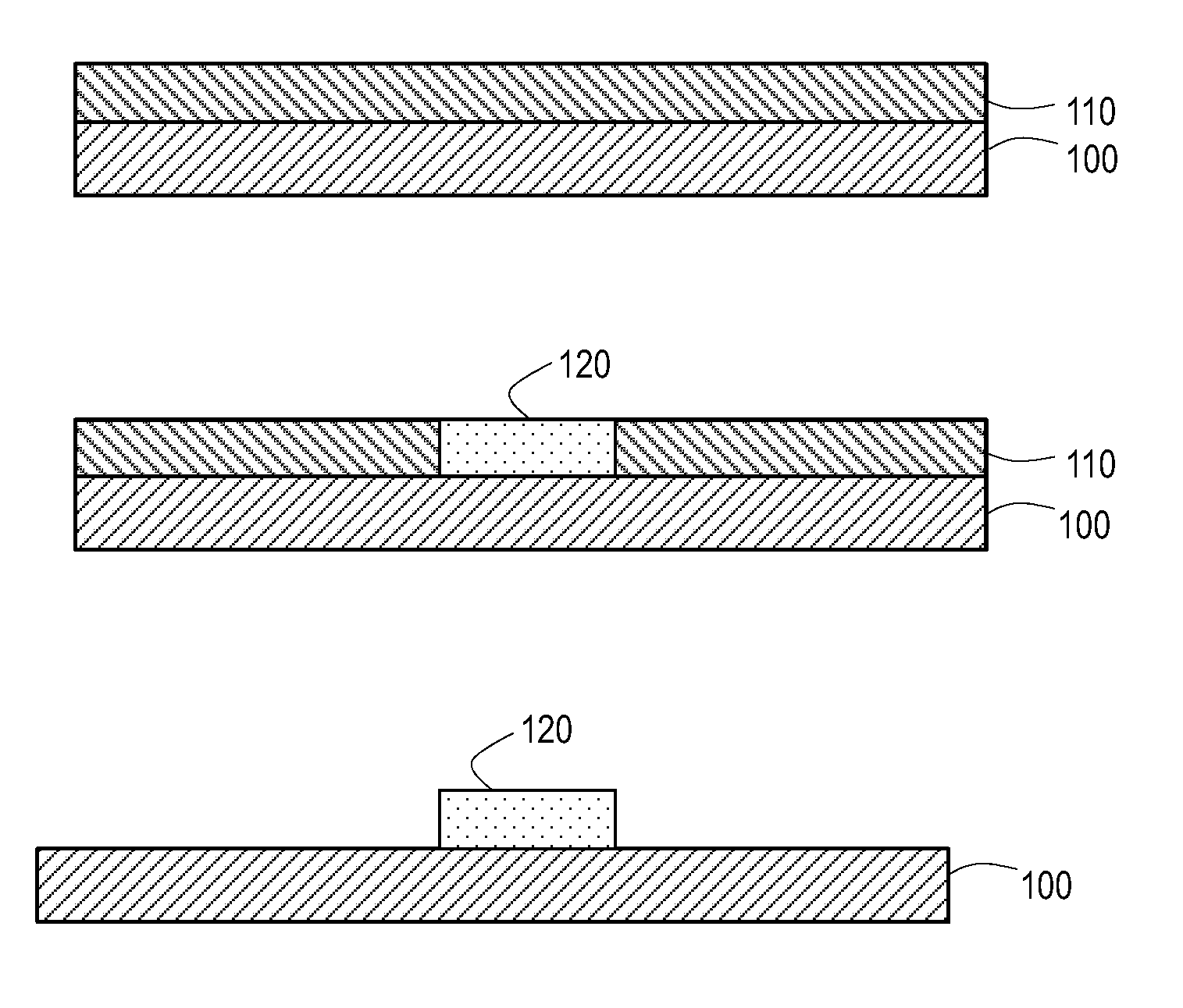
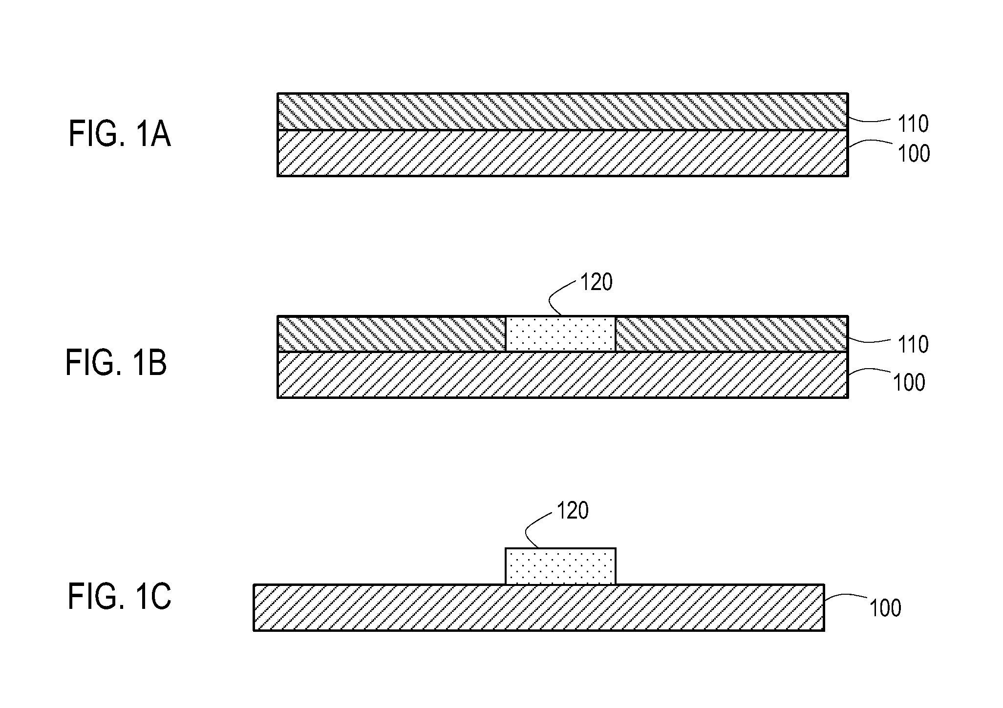
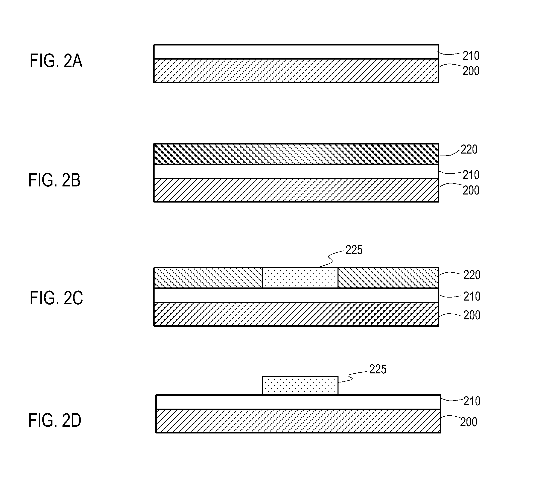
Radiation Patternable CVD Film
a patternable, cvd technology, applied in the direction of photomechanical equipment, instruments, originals for photomechanical treatment, etc., can solve problems such as problematic thinning of photoresists, and achieve the effect of plasma-enhanced chemical vapor deposition
- Summary
- Abstract
- Description
- Claims
- Application Information
AI Technical Summary
Benefits of technology
Problems solved by technology
Method used
Image

Examples
example 1
PECVD Deposition of Film Using Trisilylamine and Exposure to Radiation in Vacuum
[0074]A film was deposited using PECVD and trisilylamine as a precursor. The deposition conditions included a chamber pressure of 4 torr and a temperature of 100° C. The plasma had an RF power of 100 W. The TSA precursor was flowed at a rate of 200 sccm, while nitrogen and hydrogen were each flowed at a rate of 1000 sccm.
[0075]The deposited film was then exposed to an e-beam at 25 μC / cm2. Development consisted of puddle development for 60 seconds in a 0.26 normal TMAH solution in water.
[0076]The results showed that the film was sensitive to e-beam exposure carried out in a vacuum. The exposed film was also able to be developed using TMAH. FIGS. 3A and B are representations of optical microscope images taken of the film exposed to the e-beam before (FIG. 3A) and after (FIG. 3B) development. As seen in FIG. 3A, after exposure to the e-beam, a color change was observed in the portion of the film exposed 310...
example 2
PECVD Deposition of TSA and Exposure to Radiation in Presence of Oxygen
[0078]A film was deposited using plasma enhanced chemical vapor deposition. The film stack was comprised of 400 Angstroms of photoresist on 4000 Angstroms of APF. Film deposition was carried out at 4 torr of chamber pressure and at 100 C. The precursor was TSA, and was flowed at 200 sccm. The carrier plasma was a plasma containing argon flowed at 2000 sccm and had an RF value of 100 W. Plate spacing was 300 mil. The deposited film was then exposed to 25 mJ of 193 nm light. Development consisted of puddle development for 60 seconds in a 0.26 normal TMAH solution in water. After development, the film was etched using an oxygen-based plasma.
[0079]The deposited film demonstrated patterning using conventional photoresist processing equipment and chemicals. The film also demonstrated utility as a hard mask for etch transfer of features into the substrate.
[0080]FIG. 5 is FTIR spectra of film characterization of the depo...
PUM
| Property | Measurement | Unit |
|---|---|---|
| size | aaaaa | aaaaa |
| size | aaaaa | aaaaa |
| wavelength | aaaaa | aaaaa |
Abstract
Description
Claims
Application Information