Photovoltaic device on polarizable materials

a photovoltaic device and polarized material technology, applied in the field of photovoltaic, can solve the problems of limited depth of depletion region, complicated manufacturing of solar cell pin-junction devices, and limited optical depth of p-n junction devices, and achieve the effect of high electric strength

Inactive Publication Date: 2012-04-26
THE ISRAEL ELECTRIC CORP LTD
View PDF0 Cites 11 Cited by
  • Summary
  • Abstract
  • Description
  • Claims
  • Application Information

AI Technical Summary

Problems solved by technology

Unfortunately the depth of the depletion region is limited due to fundamental physical limitation so p-n junction devices have limited optical depth.
More advanced solar cells employ pin-junctions instead of p-n junctions to increase the optical depth, however manufacturing of solar cell pin-junctions is much more complicated.
An intrinsic disadvantage of this cell is diminishing of the electrical field produced by the electrets due to screening caused by the conducting collecting electrode which separates the depleted region from the bulk region confined by the electrodes.
Furthermore, since this solar cell employs crystalline silicon as the photo active material, its manufacturing cost is high due to the significant cost of production of crystalline silicon of a high degree of purity.
This is a common problem in the manufacture of crystalline semiconductor solar cells that inhibits their wide use.
Therefore they have the same disadvantages as cells produced from crystalline materials, i.e. Limited optical depth due to limited size of depletion region, low (˜104-105 V / cm) fields inside the depletion region, low charge carrier mobility, and large recombination rates.
Characteristic value of the field in these devices is electrical strength of 104-105 V / cm, which is insufficient for complete separation of initial excitations and for preventing recombination of the charge carriers.
Consequently, although the solar cells made of amorphous materials are much cheaper than the cells made of crystalline materials, nevertheless their disadvantage is limited power conversion efficiency, which is ˜3-5% for polymeric materials as compared with ˜10-13% for inorganic materials.
Trapping renders the transport of carriers less efficient and facilitates carrier losses during recombination.
Nevertheless it is not known to widely use this phenomenon for improving efficiency of solar cells despite the existence of a few reports on attempts to introduce a built-in electric field into polymeric solar cell devices.
Unfortunately, the quantum efficiency of this device was not compared with the efficiency of similar device based on original (non-functionalized) poly(p-phenylene vinylene); therefore it can not be concluded that the sole reason for improving the quantum efficiency is associated with the electrical field, since changing of molecular structure. of the polymer may deteriorate the performance of the device.
Unfortunately this strength of electric field is insufficient for effective separation of charge carriers and for preventing their recombination
To the best of the knowledge of the inventor, all work that is similar to that disclosed in this patent exploit a well-known anomalous photovoltaic effect that has been studied since the early 1970s and all have the same drawback, i.e. despite high output voltage achieved with photovoltaic devices based on ferroelectrics, the output current is extremely low due to high internal resistance of the ferroelectric materials.
In all cases in which the material in which photo-activity and transport of charge carriers takes place is not separated from the material that generates the electric field the result will be limited efficiency of the photovoltaic device.

Method used


Image

  • Photovoltaic device on polarizable materials
  • Photovoltaic device on polarizable materials
  • Photovoltaic device on polarizable materials

Examples


first embodiment

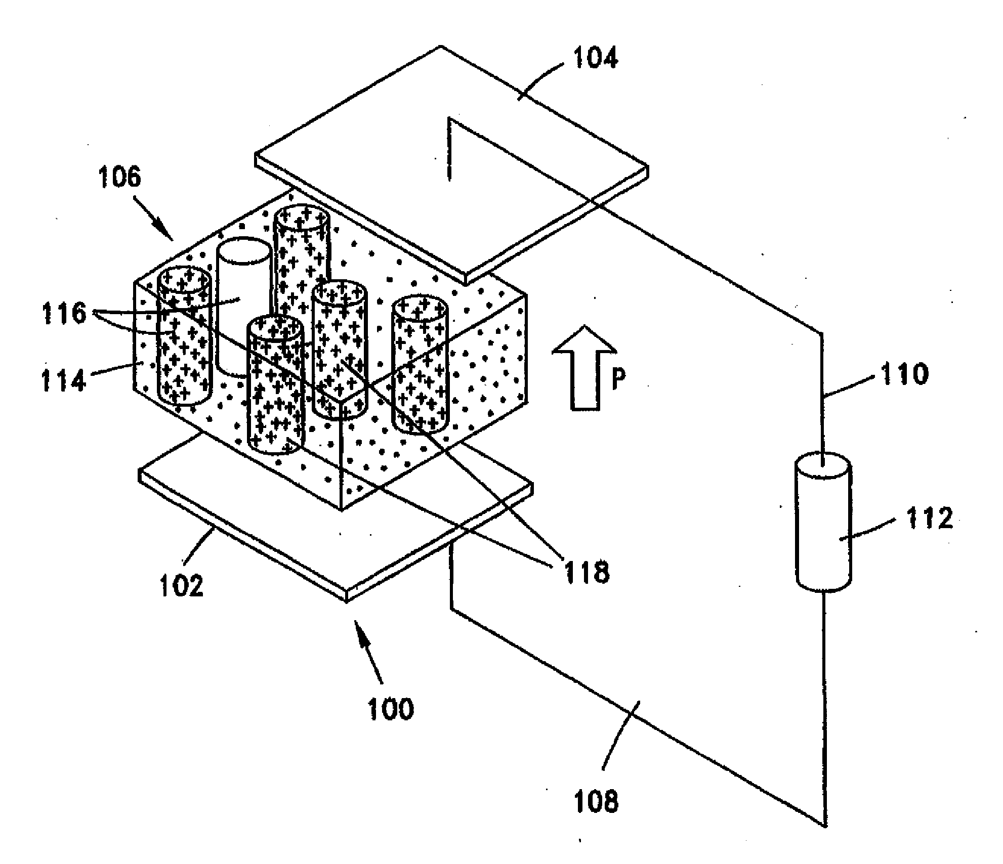
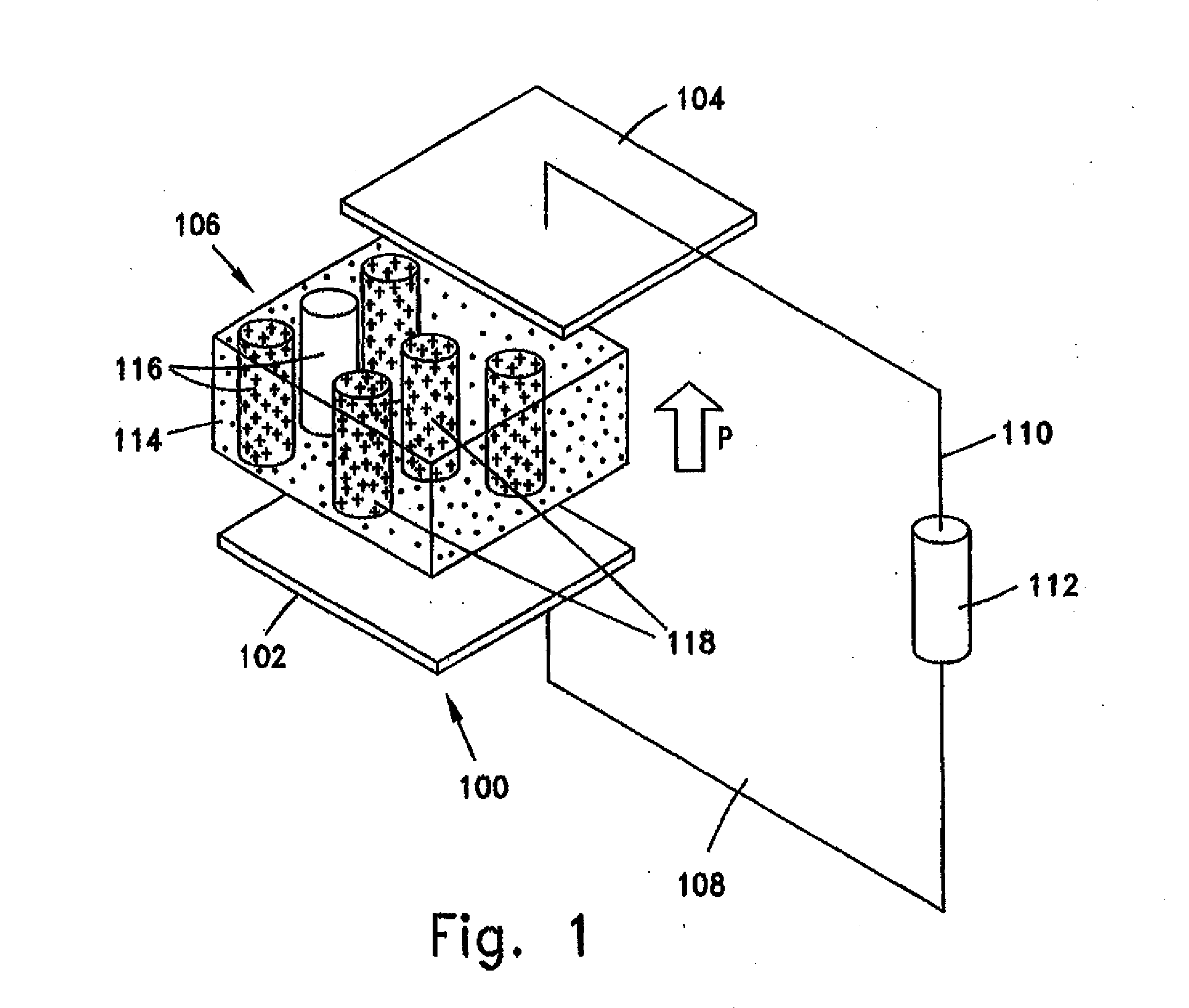
[0053]the photovoltaic device of the present invention is shown in FIG. 1. Photovoltaic device 100 comprises a pair of collecting electrodes 102, 104 and a bulk region 106 confined there between. Each of the collecting electrodes is connected by a respective wire 108, 110 to a resistive load 112. The bulk region is comprised of a matrix portion 114 in which are distributed a plurality of discrete parallel tubular-shaped channels 116. Each of the channels 116 extends through the matrix portion 114 and is entirely filled with a host portion 118. In FIG. 1, for the sake of clarity one of the channels 116 is shown empty, while the rest of the channels are shown filled with the host portion 118 configured as elongate members, e.g. rods, bars whose cross-sectional shape matches the cross-sectional shape of the channels 116.

[0054]In this embodiment of the invention the matrix portion 114 functions as a field inducing component responsible for persistent polarization directed along the dire...

second embodiment

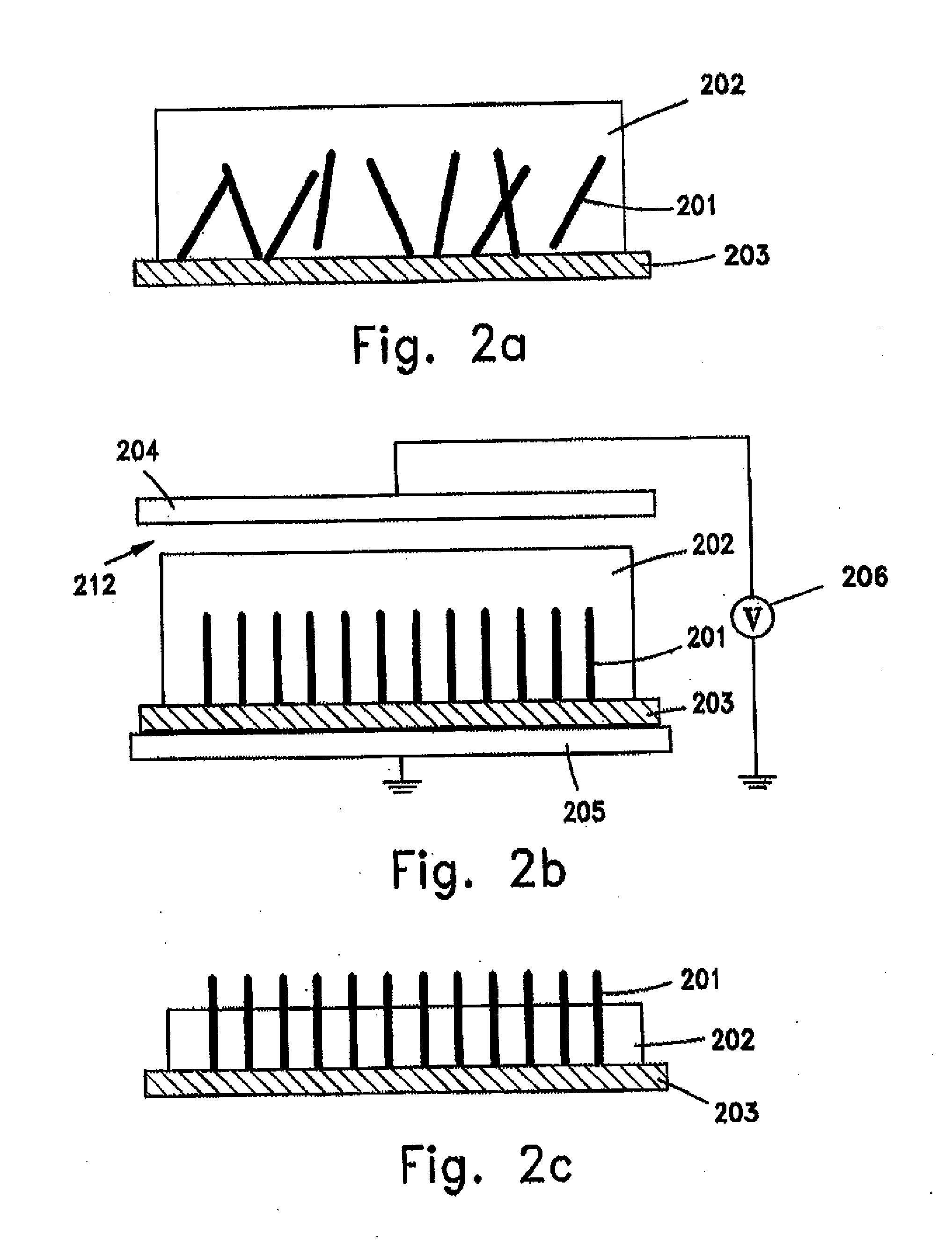
[0073]the photovoltaic device of the invention is depicted in FIG. 4. The bulk region of the device consists of a matrix portion 401 constituted in this example by the field inducing component material. The matrix portion is made of a ferroelectric material, which is capable of retaining persistent polarization in the direction shown by arrow P. The matrix portion is provided with a plurality of channels 402 that pass through it and are open at opposite sides of the bulk region. Channels 402 are filled with a photoactive material 406 of the photoactive component. The bulk region is confined between a pair of opposite collecting electrodes 403 and 404. The collecting electrodes are electrically connected with a resistive load 405. In general the structure and dimensions of this device, as well as the materials of the photoactive component and the field inducing component are similar to those already described in connection with the previous embodiment. However in contrast to the prev...

third embodiment

[0086]In the third embodiment the material of the field inducing component should be able to absorb and to keep injected charges for a long period of time (instead of persistent polarization). This technology has been known for a long time and is used to manufacture the membranes for so called electrets microphones. Organic materials that are suitable for the field inducing component are, for example, polycarbonate or PMMA. SiO2 and SiN can be named as examples of suitable inorganic materials. The injection of the charges into the materials of field inducing component is performed by the well-known corona charging process.

[0087]As an example of a method of manufacturing a device according to the third embodiment, a modification of the manufacturing method of the second embodiment (shown in FIGS. 5a to 5f) can be chosen. All steps of the method are as described herein above with the exception of the step shown in FIG. 5d, i.e. the step of filling the free space of the spatial structu...


PUM


Abstract

The invention is a photovoltaic device configured as a sandwiched structure comprising a bulk region between a pair of collecting electrodes. The bulk region comprises an electric-field inducing component and a photoactive component. The photoactive component is in electric contact with the collecting electrodes to provide a continuous conduction path for photo-generated charge carriers between the electrodes. The electric-field inducing component is adapted to provide a permanent electric field having high electric strength in the entire inter-electrode region, thereby inducing an electric field in the photoactive component. The electric-field inducing component does not participate in transport of the photo-generated charge carriers. The field inducing component can be comprised of a material that retains sustained polarization or a material that comprises and sustains a spatial distribution of electrical charges, or it can be comprised of both types of materials.

Description

CROSS REFERENCE TO RELATED APPLICATIONS[0001]This application is a continuation in part of PCT application Ser. No. PCT / IL2010 / 000351, filed on May 3, 2010, and PCT application Ser. No. PCT / IL2010 / 000386, filed on May 13, 2010.FIELD OF THE INVENTION [0002]This invention relates to conversion of electromagnetic radiation into electrical energy. More particularly the invention refers to photovoltaic or so-called solar cells that contain a photoactive component capable of converting light directly into electricity by the photovoltaic effect.BACKGROUND OF THE INVENTION[0003]Among the requirements a solar cell should comply with is sufficient optical depth, sufficient power conversion efficiency and sufficient external quantum efficiency. Accordingly many efforts are invested by designers of photovoltaic cells to improve these parameters. Traditional semiconductor solar cells employ p-n junctions for separating photo-generated electron-hole pairs by virtue of a built-in electrical field ...

Claims


Application Information

Patent Timeline
Patent Type & Authority Applications(United States)
IPC IPC(8): H01L31/06H01L31/115
CPCY02E10/549H01L51/4253Y02P70/50H10K30/30H10K30/50
Inventor PREEZANT, YEVGENI
Owner THE ISRAEL ELECTRIC CORP LTD
Why Eureka
Try Eureka