

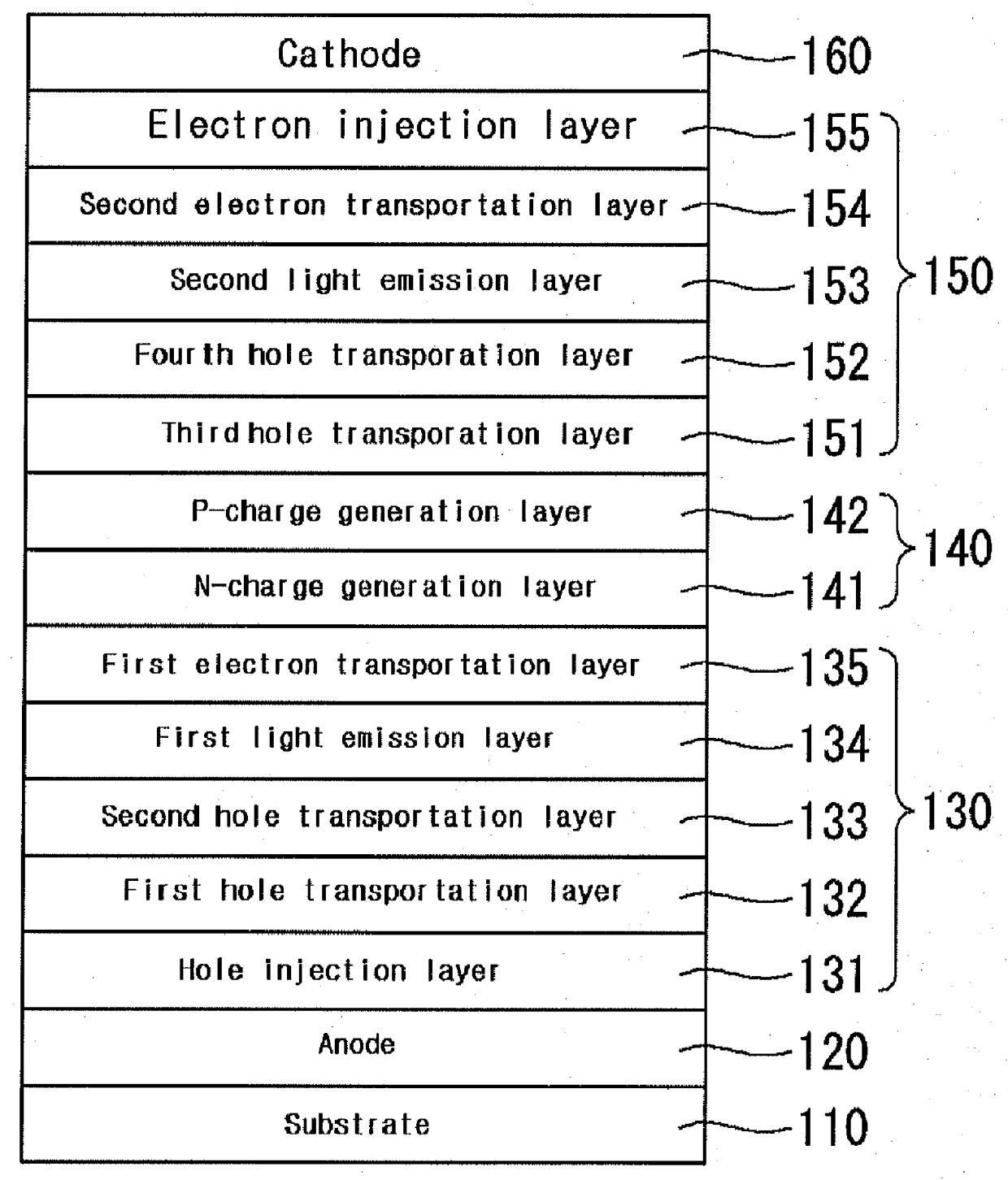
Organic light emitting diode device
a light-emitting diode and organic technology, applied in the direction of organic semiconductor devices, solid-state devices, thermoelectric devices, etc., can solve the problems of inability to meet the needs of mass production, high response speed of the emitting device, and high cos
- Summary
- Abstract
- Description
- Claims
- Application Information
AI Technical Summary
Benefits of technology
Problems solved by technology
Method used
Image

Examples
experimental example
[0054]ITO glass is patterned in such a way that the size of a light emitting area amounts to 2 mm×2 mm and the patterned ITO glass is washed. The substrate is loaded into a vacuum chamber and a base pressure of 1×10⁻⁶ torr is applied to the chamber. A hole injection layer DNTPD is coated on the ITO corresponding to the anode with a thickness of 50□. The first hole transportation layer NPD is coated with a thickness of 1600□ and the second hole transportation layer NPD is coated with a thickness of 150 □.
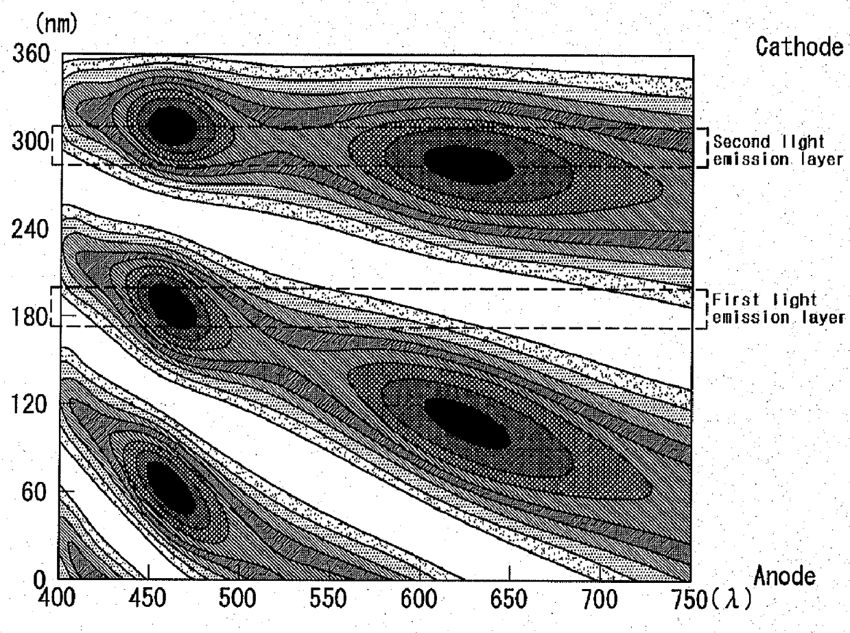
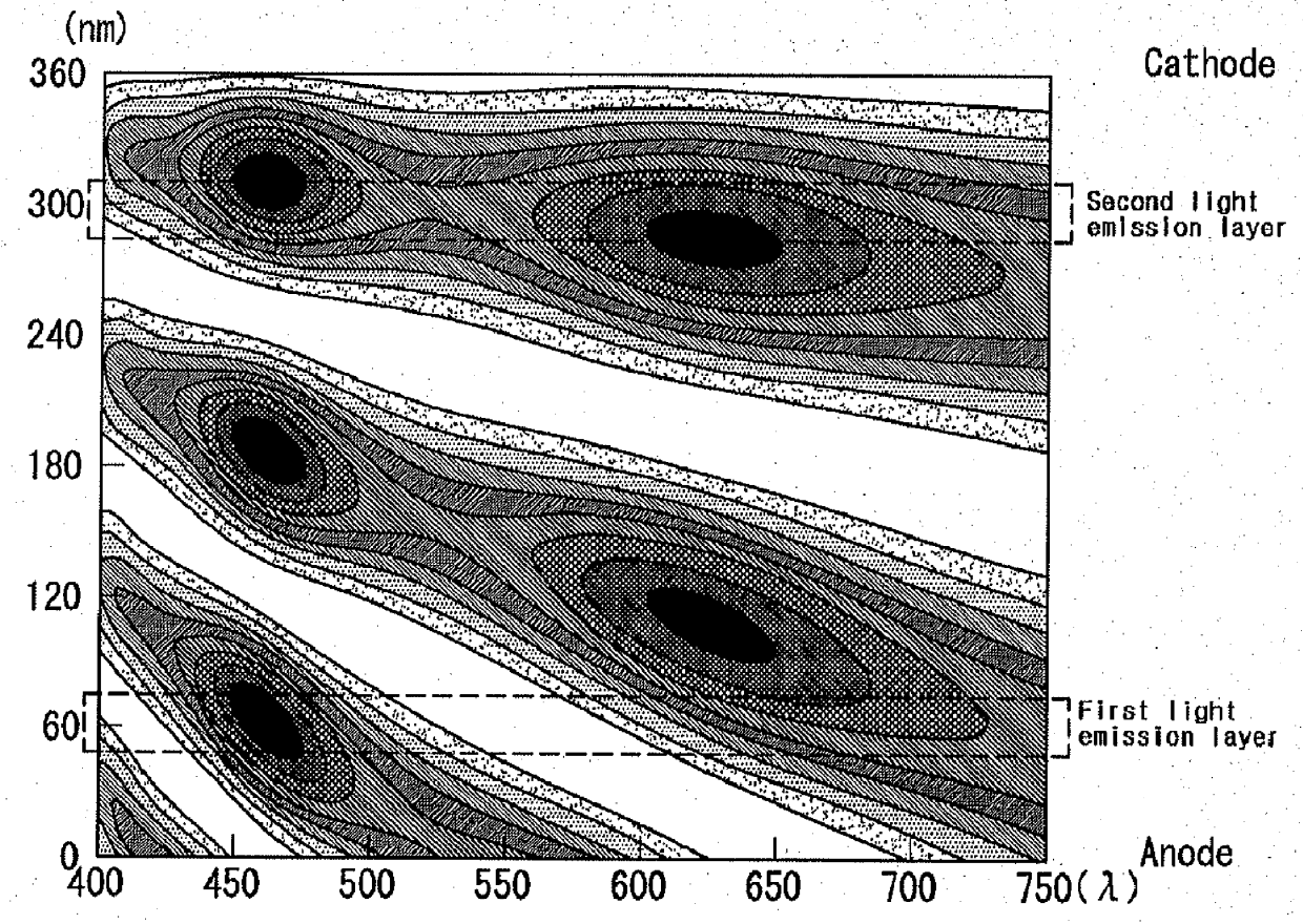
[0055]Vacuum coating with fluorescent blue dopant Ir(pFCNp)3 is applied for the host AND (9,10-di(2-naphthyl)anthracene), forming the first light emission layer with thickness of 250□. At this time, doping density of the fluorescent blue dopant was 5%. The first electron transportation layer Alq3 is coated with a thickness of 200□; N-type charge generation layer Li is coated with a thickness of 100□; and P-type charge generation layer Al is coated with a thickness of 150□.
[0056]Next,...
PUM
 Abstract
Description
Claims
Application Information