Scanning Signal Line Drive Circuit And Display Device Having The Same

a drive circuit and signal line technology, applied in the direction of digital storage, instruments, computing, etc., can solve the problems of limited picture frame area of a panel, insufficient protection of the gate driving unit, and difficulty in driving a large size liquid crystal panel by a single shift register, etc., to reduce the load capacitance per one of the clock signal main lines, suppress mutual interference, and reduce the waveform rounding of the clock signal

Active Publication Date: 2012-05-03
SHARP KK
View PDF31 Cites 31 Cited by
  • Summary
  • Abstract
  • Description
  • Claims
  • Application Information

AI Technical Summary

Benefits of technology

[0034]According to the first or tenth aspect of the present invention, the number of wire lines connecting between the clock signal main lines and each stage of the shift register decreases as compared to the conventional example. Accordingly, an area for the clock signal lines in each stage of the shift register becomes smaller. Further, as a load capacitance per one of the clock signal main lines becomes smaller as compared to the conventional example, it is possible to suppress mutual interference between the clock signals, and to reduce waveform rounding in the clock signals. Therefore, as compared to the conventional example, it is possible to downsize switching devices (for example, thin film transistors) that constitute the shift register. Moreover, it is not necessary to newly provide the shift registers with a component other than the signal lines for transmitting the clock signals between each stage of the shift register and the other shift register (or a different stage of the same shift register). As a result, it is possible to reduce a layout area for the shift registers on the panel of the display device, thereby reducing a picture-frame area of the panel.
[0035]According to the second or eleventh aspect of the present invention, the scanning signal line drive circuit provided with the shift registers operating based on the four clock signals provides the same effect as that of the first or tenth aspect.
[0036]According to the third or twelfth aspect of the present invention, it is possible to supply the clock signals to each stage of the shift register from a portion other than the clock signal main lines using relatively short signal lines. Accordingly, it is possible to achieve the scanning signal line drive circuit providing the same effect as that of the first or tenth aspect with a relatively simple configuration.
[0037]According to the fourth or thirteenth aspect of the present invention, the scanning signal line drive circuit provided with the shift registers operating based on the plurality of clock signals whose phases are displaced by 90 degrees to each other provides the same effect as that of the first or tenth aspect.
[0038]According to the fifth or fourteenth aspect of the present invention, configuring a part or all of the necessary contacts by a single contact reduces an area occupied by the contacts in each stage of the shift registers, and whereby the picture-frame area of the panel can be effectively reduced.
[0039]According to the sixth or fifteenth aspect of the present invention, it is possible to reduce a contact resistance as compared to a case in which the plurality of contacts are provided at distant positions.

Problems solved by technology

However, as described above, reduction of a picture-frame area of a panel is limited as an area for laying out the shift register increases according to the conventional structure.
However, according to the structure disclosed by Patent Document 1, increasing the number of wire lines in the gate driving unit decreases an area for applying the sealing material, resulting in insufficient protection of the gate driving unit.
However, it is difficult to drive a large size liquid crystal panel by a single shift register due to a large load, and two or more shift registers are required.

Method used


Image

  • Scanning Signal Line Drive Circuit And Display Device Having The Same
  • Scanning Signal Line Drive Circuit And Display Device Having The Same
  • Scanning Signal Line Drive Circuit And Display Device Having The Same

Examples


first embodiment

MODIFIED EXAMPLES OF FIRST EMBODIMENT

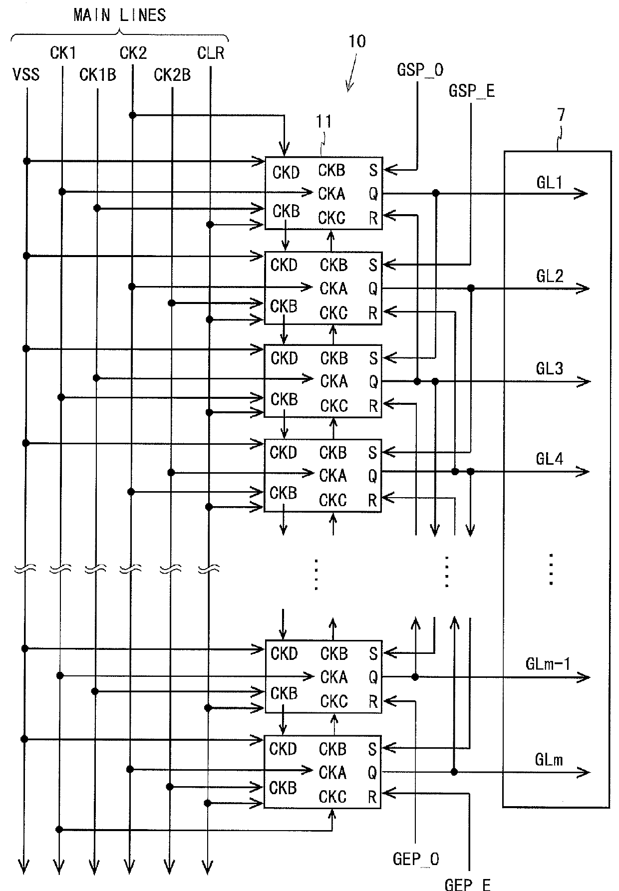
[0109]From this embodiment, modified examples as described below can be obtained. In the above description, each stage of the shift register 10 receives the clock signals that are not received from the clock signal main lines from the preceding or succeeding stage. However, the present invention is not limited to such an example. Each stage of the shift register may receive the clock signals that are not received from the clock signal main lines from a stage other than the preceding or succeeding stage of the shift register. Alternatively, each stage of the shift register may receive the first clock CKA supplied to the preceding stage as the fourth clock CKD, and the first clock CKA supplied to the succeeding stage as the third clock CKC. In addition, the bistable circuit 11 shown in FIG. 4 may include a capacitor, in place of the thin film transistor MF, between an input terminal for the third clock CKC and the second node N2.

[0110]Further, in t...

second embodiment

[0117]FIG. 17 is a block diagram illustrating a gate driver according to the second embodiment of the present invention in detail. The gate driver according to this embodiment is provided with a shift register 20 including an odd-numbered stage shift register and an even-numbered stage shift register, and main lines including clock signal main lines. The shift register 20 includes the m (=2a) bistable circuits 11 and dummy bistable circuits 21 and 22 that function as dummy stages. The dummy bistable circuits 21 and 22 do not include a thin film transistor as a switching device. The dummy bistable circuits 21 and 22 include, out of the components included in each stage of the shift register 20, only the components necessary to transmit the clock signal received from the clock signal main line.

[0118]The dummy bistable circuit 21 is provided on a side of a first stage of the shift register 20. To the dummy bistable circuit 21, the third gate clock signal CK2 is supplied as the second c...

third embodiment

[0124]FIG. 19 is a block diagram illustrating a gate driver according to the third embodiment of the present invention in detail. The gate driver according to this embodiment is provided with a shift register 30 including an odd-numbered stage shift register and an even-numbered stage shift register, and main lines including clock signal main lines. The shift register 30 includes m (=2a) bistable circuits 31 and the dummy bistable circuits 21 and 22. Each bistable circuit 31 is configured such that a function of outputting a signal Z that changes in the same manner as the state signal Q is added to the bistable circuit 11 according to the first embodiment.

[0125]FIG. 20 is a circuit diagram of the bistable circuit 31. The bistable circuit 31 is configured such that a thin film transistor MG is added to the bistable circuit 11. The thin film transistor MG outputs the first clock CKA as the signal Z while the potential of the first node N1 is at a high level. According to the first and...


PUM


Abstract

A gate driver is provided with an odd-numbered stage shift register, an even-numbered stage shift register, and main lines including clock signal main lines. In at least one example embodiment, each stage of one of the shift registers receives the first clock and the second clock from the clock signal main lines, and the third clock and the fourth clock from an adjacently provided stage of the other shift register. Each stage of the shift register can receive the second clock from a different stage of the same shift register. With this, it is possible to reduce a picture-frame area of a panel in a display device provided with a scanning signal line drive circuit having the plurality of shift registers.

Description

TECHNICAL FIELD[0001]The present invention relates to a scanning signal line drive circuit of an active matrix-type display device, and in particular to a shift register included in a scanning signal line drive circuit.BACKGROUND ART[0002]Conventionally, there is known an active matrix-type display device, in which a plurality of gate bus lines (scanning signal lines) and a plurality of source bus lines (video signal lines) are provided in a grid pattern, and a plurality of pixel formation portions are provided in matrix corresponding to respective intersection points between the signal lines. Each pixel formation portion includes a thin film transistor (Thin Film Transistor: TFT) as a switching device and a pixel capacitance for holding a pixel value. A gate terminal of the thin film transistor is connected to the gate bus line that passes the corresponding intersection point, and a source terminal of the thin film transistor is connected to the source bus line that passes the same...

Claims


Application Information

Patent Timeline
Patent Type & Authority Applications(United States)
IPC IPC(8): G09G5/00G09G3/20
CPCG02F1/13454G09G3/3266G09G3/3677G09G2310/0267G09G2310/0286G11C19/184G11C19/28
Inventor SAKAMOTO, MAYUKOIWASE, YASUAKI
Owner SHARP KK
Why Eureka
Try Eureka