Semiconductor control device for a switching regulator and a switching regulator using the semiconductor control device

a control device and switching regulator technology, applied in the direction of dc-dc conversion, power conversion systems, instruments, etc., can solve the problems of increasing the number, affecting the efficiency of the device, so as to reduce the switching loss, suppress the increase in the manufacturing cost of the device, and enhance efficiency

Active Publication Date: 2012-05-03
FUJI ELECTRIC CO LTD
View PDF1 Cites 27 Cited by
  • Summary
  • Abstract
  • Description
  • Claims
  • Application Information

AI Technical Summary

Benefits of technology

[0026]In view of the unsolved problems of the conventional examples described above, embodiments of the present invention can provide such a semiconductor control device for a switching regulator that achieves a continuous current mode in the heavy loading condition and performs bottom turning ON during resonance oscillation operation in the light loading condition without increasing the number of pins in the semiconductor control device for driving a switching element for the flyback transformer. A semiconductor control device of certain embodiments can further perform optimum switching characteristics. Embodiments of the present invention can also provide a switching regulator using such a semiconductor control device.
[0033]A semiconductor control device for a switching regulator according to embodiments of the invention can perform turning ON of a switching element connected to the primary winding of the flyback transformer at a time of a low drain voltage during an LC resonant oscillation state in the discontinuous current mode in the light loading condition without increasing the number of pins in the semiconductor control device for controlling the switching element. Therefore, the semiconductor control device of embodiments of the invention reduces the switching loss in the light loading condition to enhance efficiency while suppressing increase in the manufacturing costs of the device. Moreover, the semiconductor control device of embodiments of the invention can perform optimum switching frequency characteristics corresponding to a loading state in the light loading condition.

Problems solved by technology

However, the switching loss is rather large in the top turning ON condition in which turning ON occurs at a moment of high voltage in the resonance oscillation due to discharge of the capacitance component in the LC resonance circuit, as compared with the bottom turning ON condition in which turning ON occurs at a moment of low voltage in the resonance oscillation.
Thus, problems arise due to the increased number of pins in the semiconductor control device 110 and increased cost of the semiconductor control device 110.
Therefore, a lower loading condition generally results in a higher switching frequency, increasing energy loss.
After that time, however, the switching frequency increases with decrease of loading, this is one of the problems in the control device of Non-patent Document 1.
In the heavy loading condition, since the resonant oscillation is presumed in this conventional device, the continuous current mode operation cannot be performed.

Method used


Image

  • Semiconductor control device for a switching regulator and a switching regulator using the semiconductor control device
  • Semiconductor control device for a switching regulator and a switching regulator using the semiconductor control device
  • Semiconductor control device for a switching regulator and a switching regulator using the semiconductor control device

Examples


Embodiment Construction

[0043]Now, circuits for signal transmission in some embodiments of a switching regulator and a semiconductor control device according to embodiments of the present invention will be described in the following with reference to accompanying drawings.

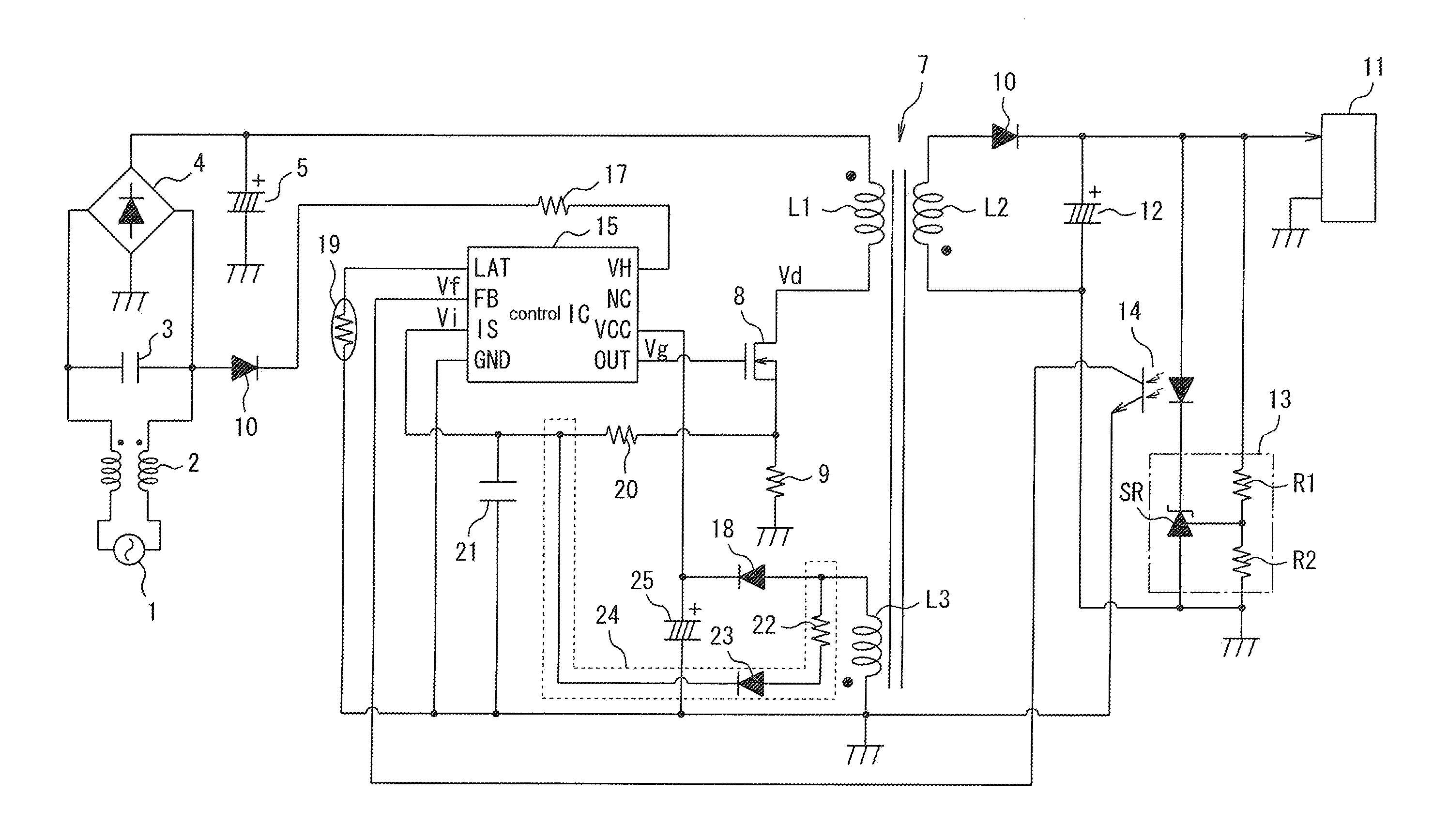
[0044]FIG. 1 is a block diagram of a switching regulator of certain embodiments of the present invention.

[0045]Referring to FIG. 1, the reference numeral 1 represents an AC power source that supplies AC power to a rectifier 4 through an input filter consisting of an inductor 2 and a capacitor 3.

[0046]The rectifier 4 converts the supplied AC voltage to a DC voltage. A smoothing capacitor 5 is connected between the positive electrode and the negative electrode of the rectifier 4. The DC output voltage from the rectifier 4 is delivered to one terminal of the primary winding L1 of the flyback transformer 7. The other terminal of the primary winding L1 is grounded through a series circuit of a switching element 8, which can be an N channel fie...


PUM


Abstract

A semiconductor control device can include a current detection signal input terminal, a feedback signal input terminal, a driving signal output terminal and a voltage adjusting circuit that delivers a voltage similar to a voltage of a primary winding of the flyback transformer to the current detection signal input terminal. The device can also include an oscillator circuit connected to the feedback signal input terminal; a one-shot circuit connected to the oscillator circuit, an RS flip-flop circuit that generates a driving signal to be delivered to the driving signal output terminal. A bottom detection section can receive a one-shot signal from the one-shot circuit, the current detection signal, and an output signal from the RS flip-flop circuit, and detect a bottom of the current detection signal to set the RS flip-flop circuit based on the detected bottom detection signal.

Description

BACKGROUND OF THE INVENTION[0001]1. Field of the Invention[0002]Embodiments of the present invention relate to semiconductor control devices for control of a switching element connected to a flyback transformer of a switching regulator.[0003]2. Description of the Related Art[0004]A flyback type switching regulator has been proposed having a circuit construction as shown in FIG. 5, in which the switching element connected to the primary winding of the flyback transformer is controlled depending on whether the load connected to the secondary winding of the flyback transformer is in a light load condition or in a heavy load condition.[0005]In the conventional example of FIG. 5, an AC voltage delivered by an AC power source 100 is converted to a DC voltage by a rectifying circuit 101, which in turn is supplied to one terminal of a primary winding L1 of a flyback transformer 102. The other terminal of the primary winding L1 is connected to the ground through a series-connected circuit co...

Claims


Application Information

Patent Timeline
Patent Type & Authority Applications(United States)
IPC IPC(8): H02M3/335
CPCH02M3/33523
Inventor SUGAWARA, TAKATO
Owner FUJI ELECTRIC CO LTD
Why Eureka
Try Eureka