Supercharge Your Innovation With Domain-Expert AI Agents!

Test apparatus

a power supply and test apparatus technology, applied in the direction of individual semiconductor device testing, semiconductor/solid-state device testing/measurement, instruments, etc., can solve the problems of deterioration in test accuracy, fluctuation in power supply voltage seriously affecting the test margin of dut, and the output impedance of the circuit is not negligible, so as to suppress the reduction of the number of product chips produced from the wafer. , the effect of reducing the number of product chips

Inactive Publication Date: 2012-05-10
ADVANTEST CORP
View PDF6 Cites 7 Cited by
  • Summary
  • Abstract
  • Description
  • Claims
  • Application Information

AI Technical Summary

Benefits of technology

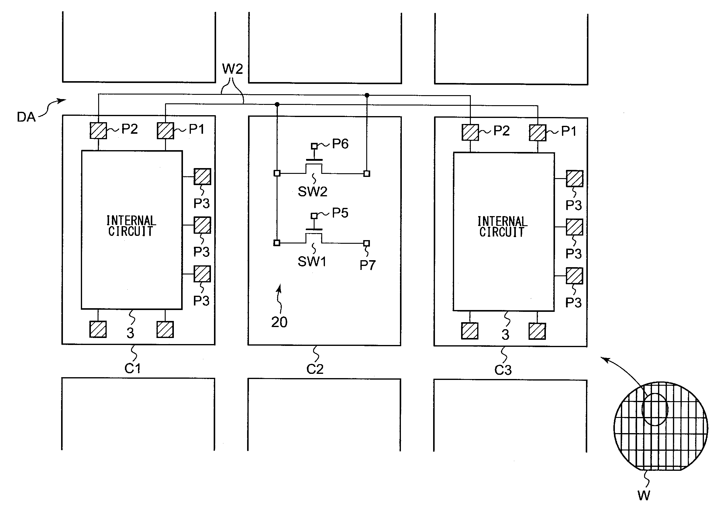
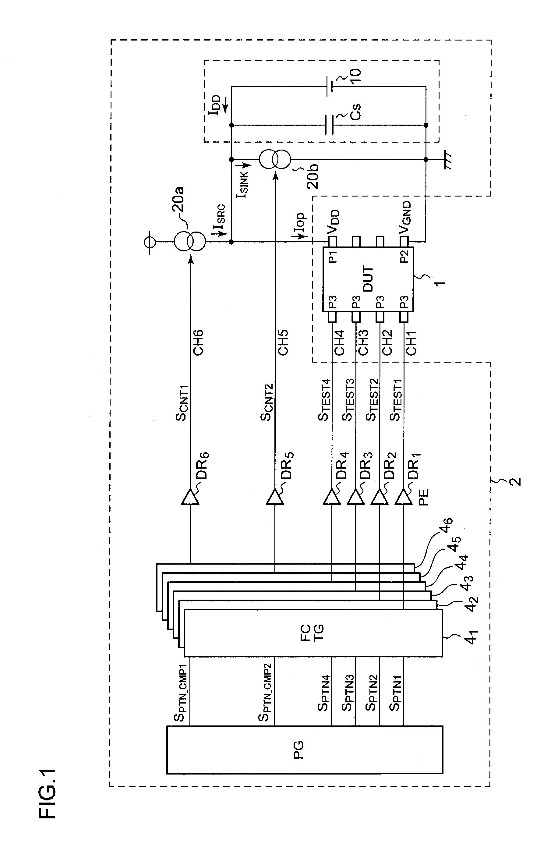
[0015]With such an embodiment, a part of the power supply compensation circuit is formed on a wafer. Thus, at the time of the probe test, such an arrangement allows the compensation pulse current to be generated on the wafer, i.e., in the vicinity of the device under test. As a result, such an arrangement is capable of providing power supply compensation while suppressing the effects of the impedance of the probes.
[0019]In a case in which the power supply compensation circuit formed within the chip is only required at the time of the probe test, the compensation pads may be formed with a sufficiently small size, thereby suppressing an increase in the chip size.
[0024]Also, at least one part of the power supply compensation circuit formed on the wafer and the compensation pad may be shared by multiple devices under test. In a case in which such power supply compensation circuit chips are arranged on a wafer, the number of product chips produced from a wafer is reduced due to the area of such power supply compensation circuit chips. With such an arrangement in which such a power supply compensation circuit chip is shared by multiple chips, such an arrangement suppresses a reduction in the number of product chips.
[0025]Also, of wiring lines respectively connected to the at least one part of the power supply compensation circuit formed on the wafer and the compensation pad, a wiring line that straddles a boundary of the chip may be formed as an aluminum wiring line. In a case in which the wiring line is arranged across the dicing line, the cross-sectional surface of the wiring line is exposed to air or moisture after the dicing. In some cases, this leads to deterioration in long-term reliability. In order to solve such a problem, such a wiring line is configured as a first layer aluminum wiring line, thereby suppressing deterioration in reliability.

Problems solved by technology

However, in actuality, such a power supply circuit has an output impedance that is not negligible.
Fluctuation in the power supply voltage seriously affects the test margin for the DUT.
Furthermore, such fluctuation in the power supply voltage affects the operations of other circuit blocks included in the test apparatus, such as a pattern generator configured to generate a pattern to be supplied to the DUT, a timing generator configured to control the pattern transition timing, etc., leading to deterioration in the test accuracy.

Method used


Image

  • Test apparatus
  • Test apparatus
  • Test apparatus

Examples


Embodiment Construction

[0037]The invention will now be described based on preferred embodiments which do not intend to limit the scope of the present invention but exemplify the invention. All of the features and the combinations thereof described in the embodiment are not necessarily essential to the invention.

[0038]In the present specification, the state represented by the phrase “the member A is connected to the member B” includes a state in which the member A is indirectly connected to the member B via another member that does not substantially affect the electric connection therebetween, or that does not damage the functions or effects of the connection therebetween, in addition to a state in which the member A is physically and directly connected to the member B. Similarly, the state represented by the phrase “the member C is provided between the member A and the member B” includes a state in which the member A is indirectly connected to the member C, or the member B is indirectly connected to the m...


PUM


Abstract

A test apparatus tests a DUT formed on a wafer. A power supply compensation circuit includes source and a sink switches each controlled according to a control signal. When the source or sink switch is turned on, a compensation pulse current is generated, and the compensation pulse current is injected into a power supply terminal of the DUT via a path that differs from that of a main power supply, or is drawn from the power supply current that flows from the main power supply to the DUT via a path that differs from that of the power supply terminal of the DUT. Of components forming the power supply compensation circuit, including the source and sink switches, a part is formed on the wafer. Pads are formed on the wafer in order to apply a signal to such a part of the power supply compensation circuit formed on the wafer.

Description

BACKGROUND OF THE INVENTION[0001]1. Field of the Invention[0002]The present invention relates to a technique for stabilizing a power supply.[0003]2. Description of the Related Art[0004]In a testing operation for a semiconductor integrated circuit that employs CMOS (Complementary Metal Oxide Semiconductor) technology (which will be referred to as the “DUT” hereafter) such as a CPU (Central Processing Unit), DSP (Digital Signal Processor), memory, or the like, electric current flows in a flip-flop or a latch included in the DUT while it operates receiving the supply of a clock. When the clock is stopped, the circuit enters a static state in which the amount of current decreases. Accordingly, the sum total of the operating current (load current) of the DUT changes over time depending on the content of the test operation, and so forth.[0005]A power supply circuit configured to supply electric power to such a DUT has a configuration employing a regulator, for example. Ideally, such a pow...

Claims


Application Information

Patent Timeline
IPC IPC(8): G01R31/26
CPCG01R31/31721G11C2029/5602G11C29/56004G01R31/318511G01R31/28H01L22/00
Inventor ISHIDA, MASAHIROWATANABE, DAISUKEKAWABATA, MASAYUKIOKAYASU, TOSHIYUKI
Owner ADVANTEST CORP
Features
  • R&D
  • Intellectual Property
  • Life Sciences
  • Materials
  • Tech Scout
  • Unparalleled Data Quality
  • Higher Quality Content
  • 60% Fewer Hallucinations
Learn More