Miniaturized Spring Contact

Inactive Publication Date: 2012-05-17
LUO DR QI
View PDF0 Cites 13 Cited by
  • Summary
  • Abstract
  • Description
  • Claims
  • Application Information

AI Technical Summary

Benefits of technology

[0010]In general, it is the object of the present invention to provide a miniaturized spring contact and an array of such miniaturized spring cont

Problems solved by technology

This poses difficulties for traditional epoxy ring contact and blade contact technologies, and also poses desires for improvement and new designs of the micro-spring contact technology.
However, this type of spring contacts intrinsically suffers from some process deficiencies.
Second, the released springs, prior to the electroplating, are fragile and easy to fracture during the following process.
Third, the large tension force app

Method used


Image

  • Miniaturized Spring Contact
  • Miniaturized Spring Contact
  • Miniaturized Spring Contact

Examples


Embodiment Construction

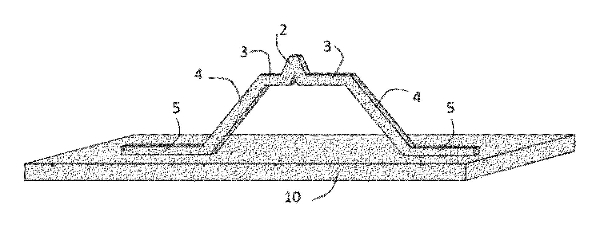
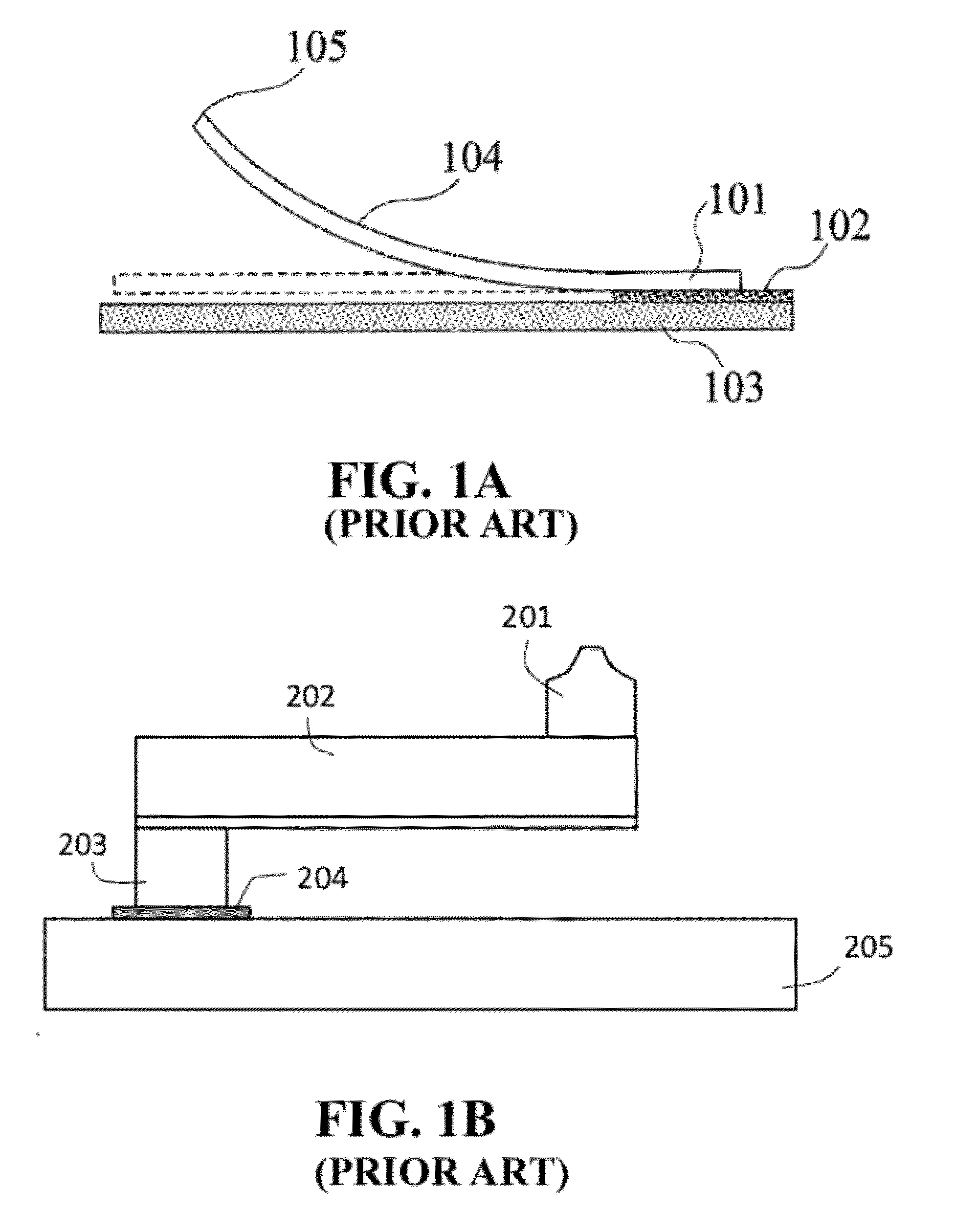
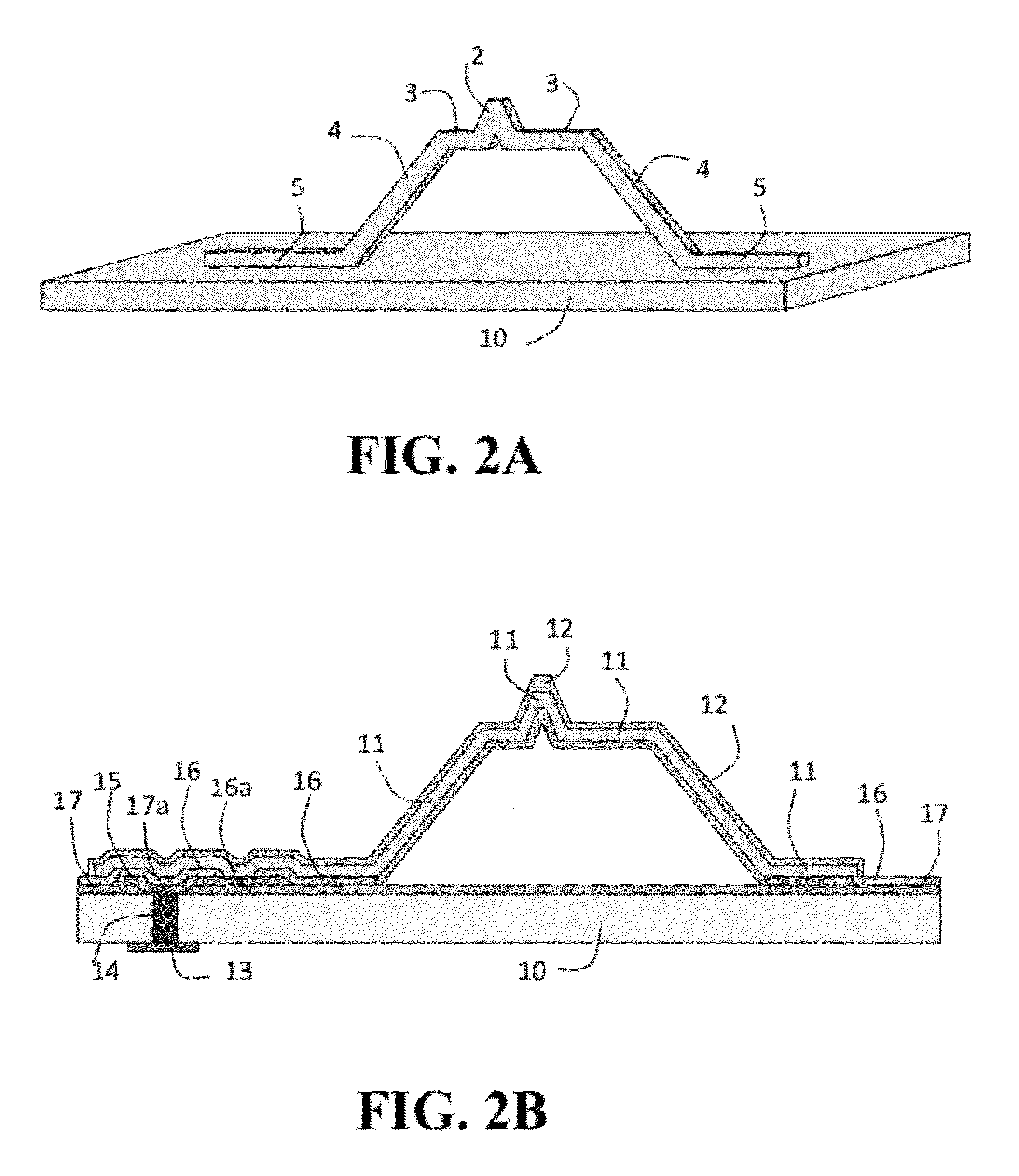
[0028]The following detailed description is directed to certain specific embodiments of the invention. In the description, reference is made to the drawings wherein like parts may be assigned with like numerals throughout. Also, for ease of description, the dimensions of the parts are not to the scale. Because of this, important dimensions are given in values throughout the whole description of the embodiments.

[0029]The present invention provides a spring contact that possesses pre-determined mechanical strength and electric conductivity. Normally, at non-operational state, a spring contact is at un-stressed condition and no deformation is created; in the situation that the spring contact is pressed against the testing pad of a semiconductor device on a semiconductor wafer, the spring contact elastically deforms, and this deformation provides certain required force to make a good mechanical contact to the testing pad. Once a stable mechanical and electrical contact to the testing pa...


PUM

PropertyMeasurementUnit
Widthaaaaaaaaaa
Widthaaaaaaaaaa
Widthaaaaaaaaaa

Abstract

A method of manufacturing an array of miniaturized spring contacts is disclosed. The invention teaches a symmetric design of the spring contact with two anchoring traces at each side of the spring contact, and teaches a method of forming the spring contact with a continuo us, zero-stress core member throughout the entire body of the spring contact; besides these, the invention enables easy manufacturing of integrated fine pitch spring contact arrays, allows fabrication of such spring contact arrays with extremely uniform spring height and good electrical and mechanical properties.

Description

FIELD OF THE INVENTION[0001]The present invention relates to miniaturized spring contacts manufactured using micro-electronic-mechanical-systems (MEMS) fabrication techniques, and particularly to miniaturized spring contacts in application of bonding and testing of semiconductor integrated circuitry (IC) devices.BACKGROUND OF THE INVENTION[0002]Semiconductor devices, such as integrated circuitry (IC), are massively manufactured by fabricating hundreds or even thousands of identical circuitry on a single semiconductor wafer, and hundreds or thousands of such wafers daily using photolithography in combination with various other material additive and removal processes. After being fabricated, these semiconductor devices are subsequently electrically connected to external electrical testers through electrical contact devices, such as probe cards, so that they can be tested.[0003]An electrical contact device, such as probe card, is an integral part of connecting device to connect IC devi...

Claims


Application Information

Patent Timeline
IPC IPC(8): H01R9/00
CPCG01R1/06716G01R3/00H01L21/4853H01L23/49811Y10T29/49147H01L2924/0002Y10T29/49149Y10T29/49204H01L2924/00
Inventor LUO, QI
Owner LUO DR QI
Why Eureka
Try Eureka