Film for the backside of flip-chip type semiconductor, dicing tape-integrated film for the backside of semiconductor, method of manufacturing film for the backside of flip-chip type semiconductor, and semiconductor device

a technology of flip-chip type semiconductor and backside, which is applied in the direction of film/foil adhesives, synthetic resin layered products, transportation and packaging, etc., can solve problems such as lack of productivity, and achieve the effect of suppressing the increase of manufacturing steps

Inactive Publication Date: 2012-05-24
NITTO DENKO CORP
View PDF4 Cites 36 Cited by
  • Summary
  • Abstract
  • Description
  • Claims
  • Application Information

AI Technical Summary

Benefits of technology

[0018]Because the film for the backside of a flip-chip type semiconductor manufactured according to the above-described configuration has an electromagnetic wave shielding layer, it is not necessary to add a step of forming the electromagnetic wave shielding layer when manufacturing a semiconductor device. That is, the electromagnetic wave shielding layer can be provided on the backside of the semiconductor element in one step without requiring multiple steps such as a step of forming the adhesive layer on the backside of the semiconductor element and a step of forming the electromagnetic wave shielding layer. As a result, an increase of the manufacturing steps can be suppressed as much as possible.

Problems solved by technology

Therefore, there has been a problem of lack of productivity.

Method used


Image

  • Film for the backside of flip-chip type semiconductor, dicing tape-integrated film for the backside of semiconductor, method of manufacturing film for the backside of flip-chip type semiconductor, and semiconductor device
  • Film for the backside of flip-chip type semiconductor, dicing tape-integrated film for the backside of semiconductor, method of manufacturing film for the backside of flip-chip type semiconductor, and semiconductor device
  • Film for the backside of flip-chip type semiconductor, dicing tape-integrated film for the backside of semiconductor, method of manufacturing film for the backside of flip-chip type semiconductor, and semiconductor device

Examples


example 1

Production of Adhesive Layer A

[0167]Adhesive composition solutions having a concentration of 23.6% by weight were obtained by dissolving the following (a) to (f) in methylethylketone.

[0168](a) 100 parts of an acrylic ester polymer having ethyl acrylate-methyl methacrylate as a main component (Paracron W-197CM manufactured by Negami Chemical Industries Co., Ltd.)

[0169](b) 242 parts of an epoxy resin 1 (Epicoat 1004 manufactured by Japan Epoxy Resin Co., Ltd.)

[0170](c) 220 parts of an epoxy resin 2 (Epicoat 827 manufactured by Japan Epoxy Resin Co., Ltd.)

[0171](d) 489 parts of a phenol resin (Milex XLC-4L manufactured by Mitsui Chemicals, Inc.)

[0172](e) 660 parts of spherical silica (SO-25R manufactured by Admatechs Co., Ltd.)

[0173](f) 3 parts of a thermosetting catalyst (C11-Z manufactured by Shikoku Chemicals Corporation)

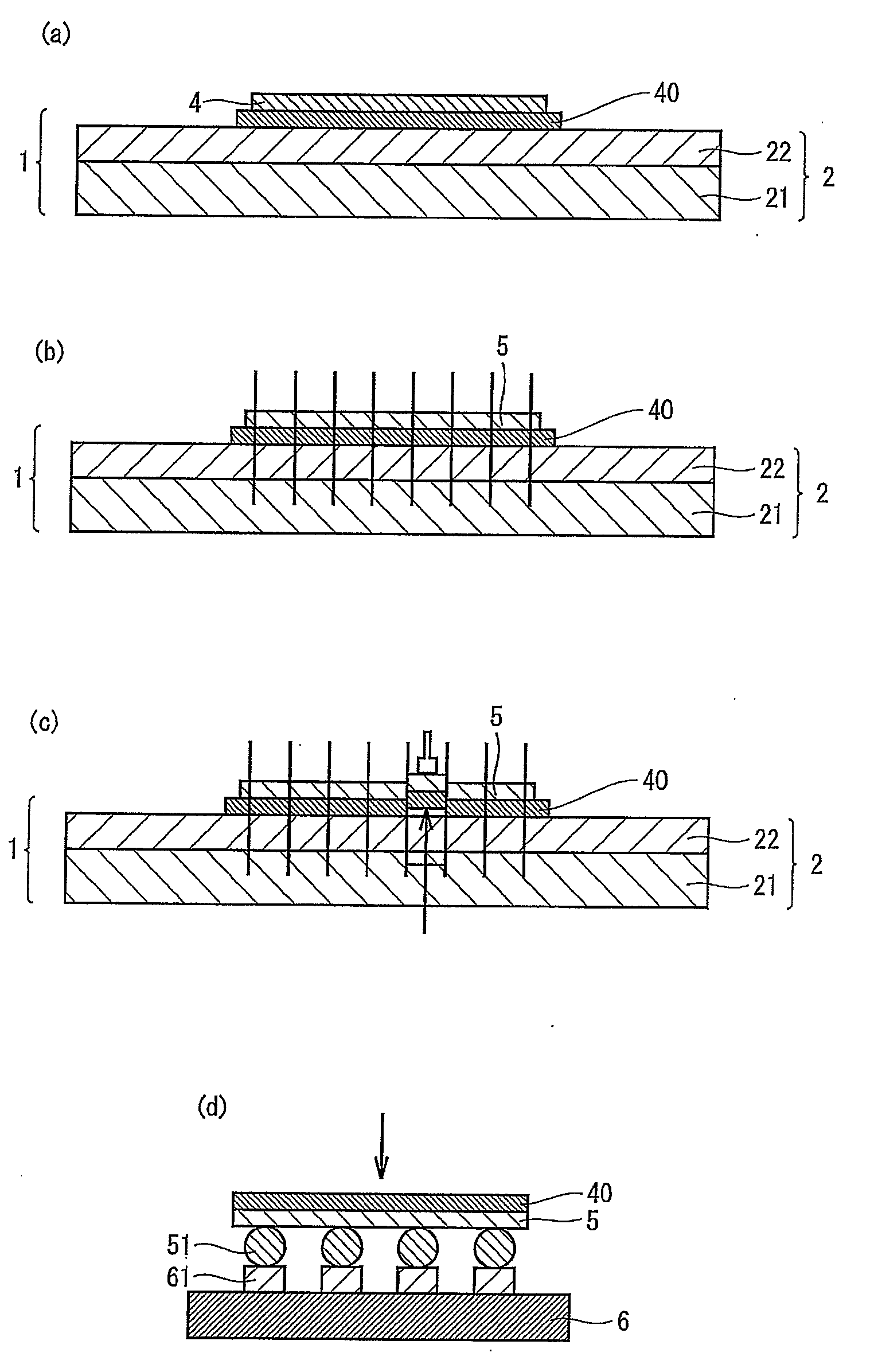
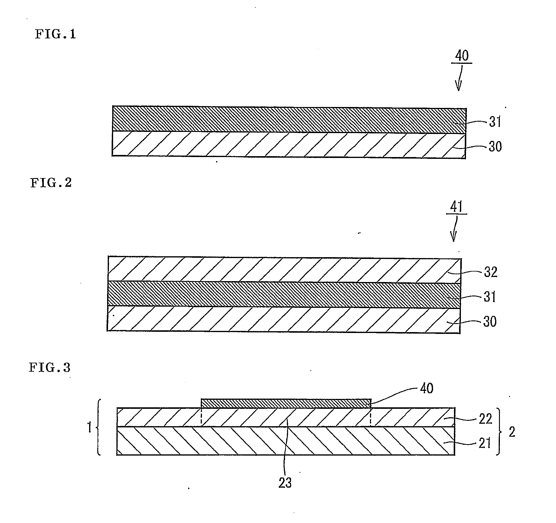
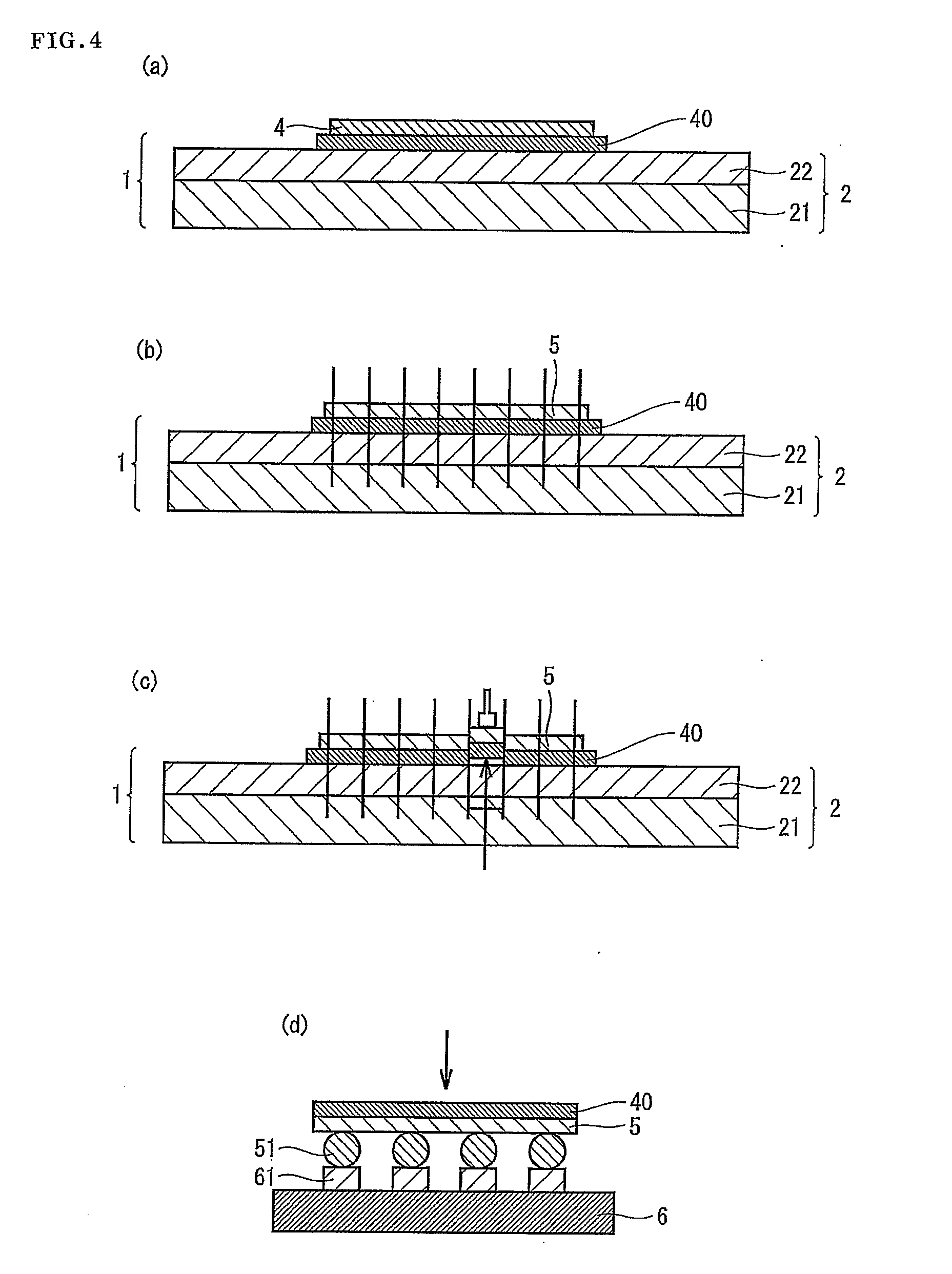
[0174]An adhesive layer A having a thickness of 60 μm was produced by applying this adhesive composition solution onto a release-treated film (a release liner) made...

example 2

Production of Film for the Backside of Semiconductor

[0182]A film for the backside of semiconductor having a thickness of 108 μm was produced by pasting a SUS304 (stainless steel) foil having a thickness of 38 μm between the adhesive layer A and the adhesive layer B under conditions of a temperature of 80° C., a pasting pressure of 0.3 MPa, and a pasting speed of 10 mm / sec. The SUS304 foil has a function as an electromagnetic wave shielding layer.

example 3

Production of Film for the Backside of Semiconductor

[0183]An aluminum layer having a thickness of 500 nm was formed on the adhesive layer A by a sputtering method using a sputtering machine (SH-550 manufactured by ULVAC, Inc.). The sputtering conditions were as follows.

(Sputtering Conditions)

Target: Aluminum

[0184]Discharge power: DC 600 W (Output density 3.4 W / cm2)

System pressure: 0.56 Pa

Ar flow rate: 40 sccm

Substrate temperature: not heated

Film forming rate: 20 nm / min

[0185]Then, a film for the backside of semiconductor having a thickness of 70.5 μm was produced by pasting the adhesive layer B onto an aluminum layer under conditions of a temperature of 80° C., a pasting pressure of 0.3 MPa, and a pasting speed of 10 mm / sec. The aluminum layer has a function as an electromagnetic wave shielding layer.


PUM

PropertyMeasurementUnit
transmittanceaaaaaaaaaa
electric conductivityaaaaaaaaaa

Abstract

An electromagnetic wave shielding layer can be provided on the backside of a semiconductor element that is flip-chip connected to an adherend, and a semiconductor device having the electromagnetic wave shielding layer can be manufactured without deteriorating productivity. The present invention provides a film for the backside of a flip-chip type semiconductor to be formed on the backside of a semiconductor element that is flip-chip connected to an adherend, having an adhesive layer and an electromagnetic wave shielding layer.

Description

BACKGROUND OF THE INVENTION[0001]1. Field of the Invention[0002]The present invention relates to a film for the backside of a flip-chip type semiconductor and a dicing tape-integrated film for the backside of a semiconductor. The film for the backside of a flip-chip type semiconductor is used to protect the backside of a semiconductor element such as a semiconductor chip, and to improve the strength. The present invention also relates to a method of manufacturing a film for the backside of a flip-chip type semiconductor, and a flip-chip mounted semiconductor device.[0003]2. Description of the Related Art[0004]In recent years, there have been increasing demands for thickness reduction and size reduction of semiconductor devices and packages thereof. Because of that, a flip-chip type semiconductor device has been broadly used in which a semiconductor element such as a semiconductor chip is mounted on a substrate by flip-chip bonding (flip-chip connection) as a semiconductor device and...

Claims


Application Information

Patent Timeline
Patent Type & Authority Applications(United States)
IPC IPC(8): H01L23/552B05D5/10B32B27/00
CPCH01L21/563Y10T428/28H01L23/544H01L23/552H01L2221/68327H01L2221/68377H01L2221/68386H01L2224/13111H01L2224/13113H01L2224/13116H01L2224/13118H01L2224/13139H01L2224/13144H01L2224/13147H01L2224/16225H01L2224/16245H01L2224/73204H01L2224/81193H01L2224/81815H01L2224/831H01L2224/83862H01L2924/01019H01L2924/01037H01L2924/01055H01L2924/01079H01L21/6836H01L2924/00C09J7/00H01L21/78
Inventor UENDA, DAISUKEMATSUMURA, TAKESHIINOUE, KOICHIMORITA, MIKI
Owner NITTO DENKO CORP
Why Eureka
Try Eureka