Thin-film solar cell and manufacturing method thereof

a technology applied in the field manufacturing methods thereof, can solve the problems of two types of thin-film solar cells from being mass-produced, long life time, and high cost, and achieve the effects of reducing grain boundaries, reducing defects in crystals, and effective control of conten

Inactive Publication Date: 2012-05-31
NEXPOWER TECH
View PDF1 Cites 30 Cited by
  • Summary
  • Abstract
  • Description
  • Claims
  • Application Information

AI Technical Summary

Benefits of technology

[0012]Therefore, with the coevaporation process and the thermal annealing process provided in the thin-film solar cell and the manufacturing method thereof according to the second embodiment of the present invention, it is able to effectively control a content of the alkali metal in the absorber layer, help the crystal growth in the absorber layer to form crystals with relatively large grains, red...

Problems solved by technology

This type of absorber layer has excellent anti-interference ability and radiation-resistant ability, and accordingly, has long life time.
However, since indium and gallium used in the CuInSe2 t...

Method used


Image

  • Thin-film solar cell and manufacturing method thereof
  • Thin-film solar cell and manufacturing method thereof
  • Thin-film solar cell and manufacturing method thereof

Examples


Embodiment Construction

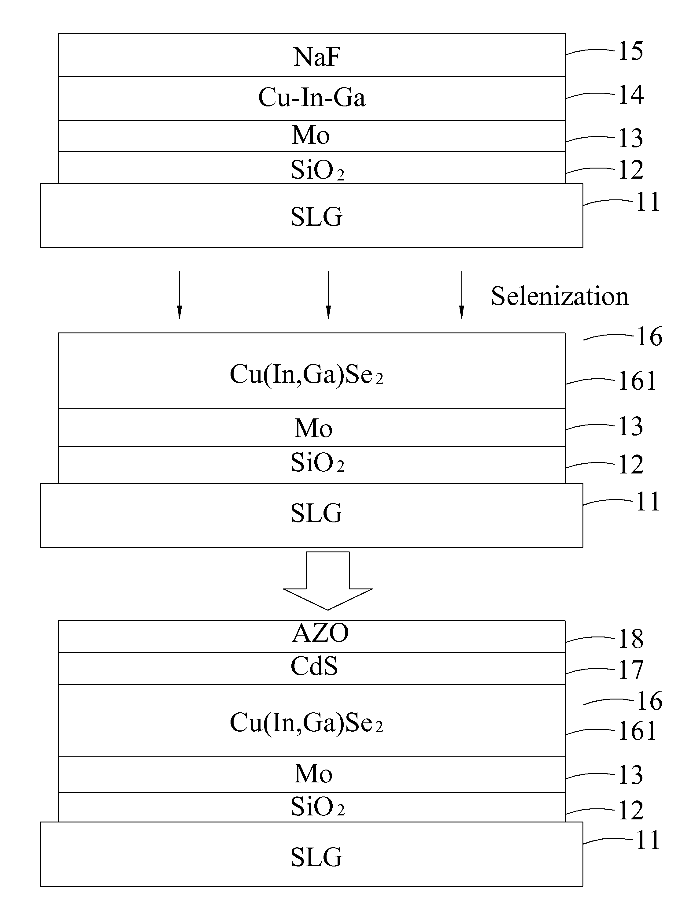
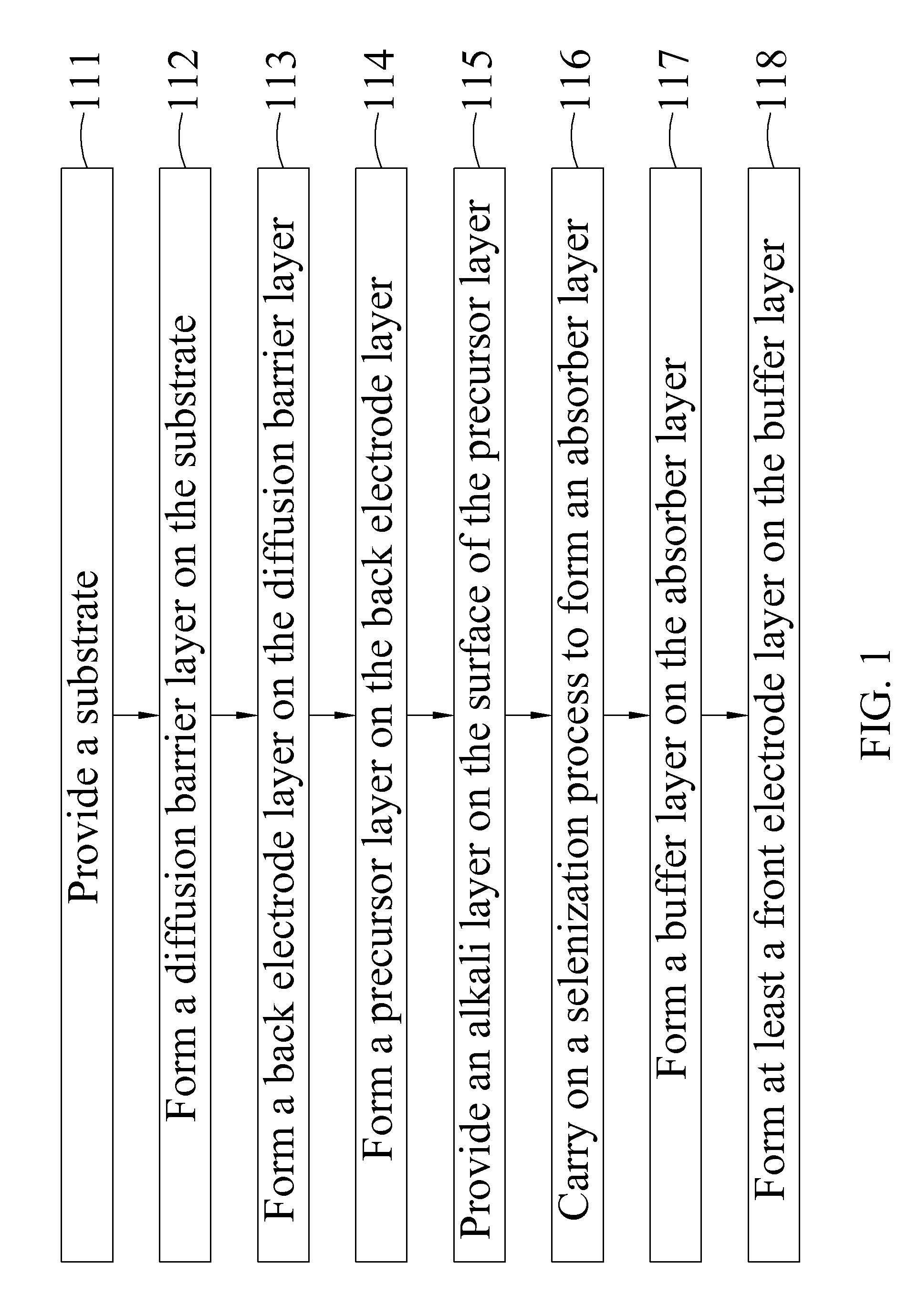
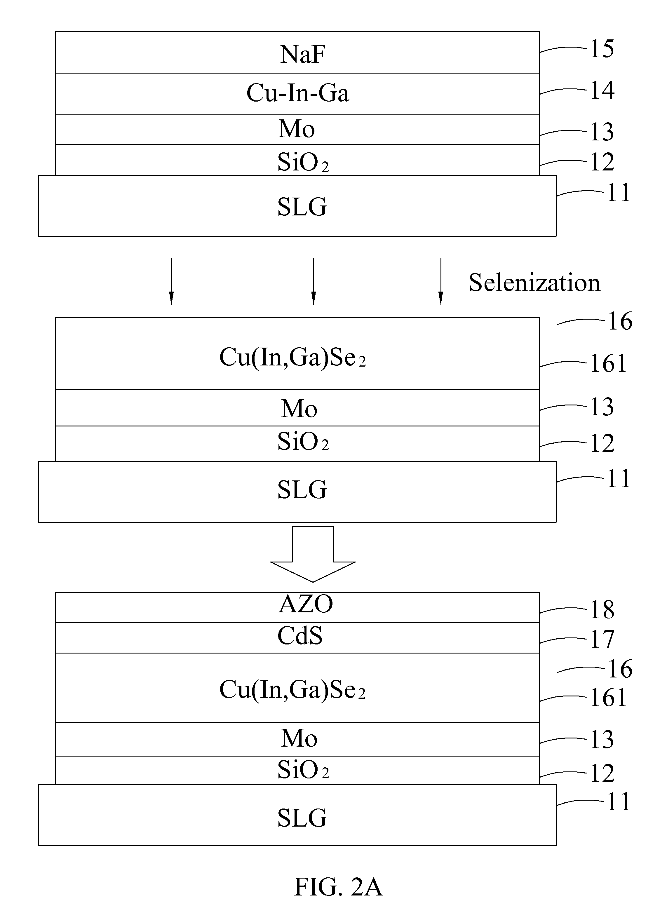
[0020]The present invention discloses a thin-film solar cell and a manufacturing method thereof. Since the principle of photovoltaic conversion based on which the solar cell of the present invention works is known by one of ordinary skill in the art, it is not described in details herein. Meanwhile, it is understood the accompanying drawings are illustrated only for assisting in describing the present invention and is not necessarily in compliance with the exact or precise size proportion and part arrangement of a real product manufactured through implementing the present invention.

[0021]To achieve the aforesaid objects, a first preferred embodiment of the present invention is a method of manufacturing a thin-film solar cell. Please refer to FIGS. 1 and 2A. The method of manufacturing a thin-film solar cell according to the first preferred embodiment of the present invention includes the following steps:

[0022]Step 111: Providing a substrate 11. In the illustrated first preferred emb...


PUM


Abstract

A thin-film solar cell and a manufacturing method thereof are disclosed. The method of manufacturing the thin-film solar cell includes the steps of providing a substrate; forming a diffusion barrier layer on the substrate; forming a back electrode layer on the diffusion barrier layer; forming a precursor layer on the back electrode layer, and the precursor layer including at least Cu, In and Ga; providing an alkali layer on an upper surface of the precursor layer, and the alkali layer being formed of Li, Na, K, Rb, Cs, or an alkali metal compound; providing a selenization process for the precursor layer and the alkali layer to form an absorber layer, such that an atomic percentage concentration of the alkali metal in the absorber layer is ranged between 0.01%˜10%; forming at least a buffer layer on the absorber layer; and forming at least a front electrode layer on the buffer layer.

Description

FIELD OF THE INVENTION[0001]The present invention relates to a thin-film solar cell and manufacturing method thereof, and more particularly to a thin-film solar cell and manufacturing method thereof, in which an absorber layer with a chalcopyrite Cu(In, Ga)Se2 structure is formed and an absorber layer with a Cu(In, Ga)S2 or Cu(In, Ga)(Se,S)2 structure is further formed on a surface of the chalcopyrite Cu(In, Ga)Se2 structure.BACKGROUND OF THE INVENTION[0002]A solar cell is mainly a p-n junction semiconductor structure, which directly converts absorbed light energy into electric energy via a process known as photovoltaic effect. In recent years, to satisfy the demands for reducing material use, the development of thin-film solar cell has become a main trend in the solar cell field. While the thin-film solar cell can be advantageously produced at relatively low manufacturing cost, it needs improvement in terms of the efficiency, stability and production yield thereof.[0003]Most of the...

Claims


Application Information

Patent Timeline
IPC IPC(8): H01L31/0264H01L31/18H01L31/0272
CPCH01L31/0322Y02E10/541H01L31/0749Y02P70/50
Inventor YANG, CHIEN-PANGYEH, CHIH-HUNG
Owner NEXPOWER TECH
Why Eureka
Try Eureka