Oxide MEMS beam

a beam and mems technology, applied in the field of micro electromechanical systems, can solve the problems of beam bending up or down, unsatisfactory mems beam bending,

Inactive Publication Date: 2012-05-31
IBM CORP
View PDF3 Cites 79 Cited by
  • Summary
  • Abstract
  • Description
  • Claims
  • Application Information

AI Technical Summary

Benefits of technology

[0007]A first aspect of the disclosure provides a semiconductor structure, comprising: a beam positioned within a sealed cavity, the beam comprising: an upper insulator layer comprising one or more layers; and a lower insulator layer comprising one or more layers, wherein a composite stress of the upper insulator layer is different than a composite stress of the lower insulator layer, such that the beam bends.

Problems solved by technology

During wafer processing, variation in film thickness or stress can induce undesirable MEMS beam bending.
In addition, during operation, a MEMS beam bridge may be exposed to varying temperatures that may cause the beam to bend up or down.

Method used


Image

  • Oxide MEMS beam
  • Oxide MEMS beam
  • Oxide MEMS beam

Examples


Embodiment Construction

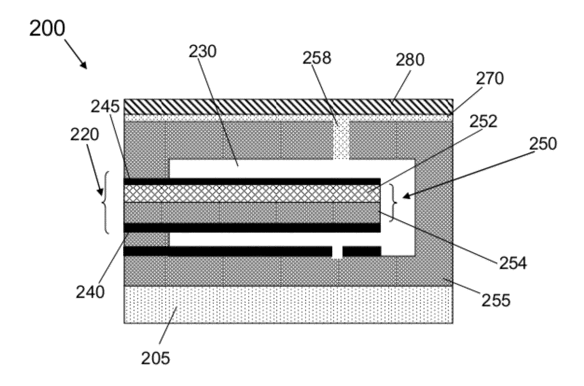
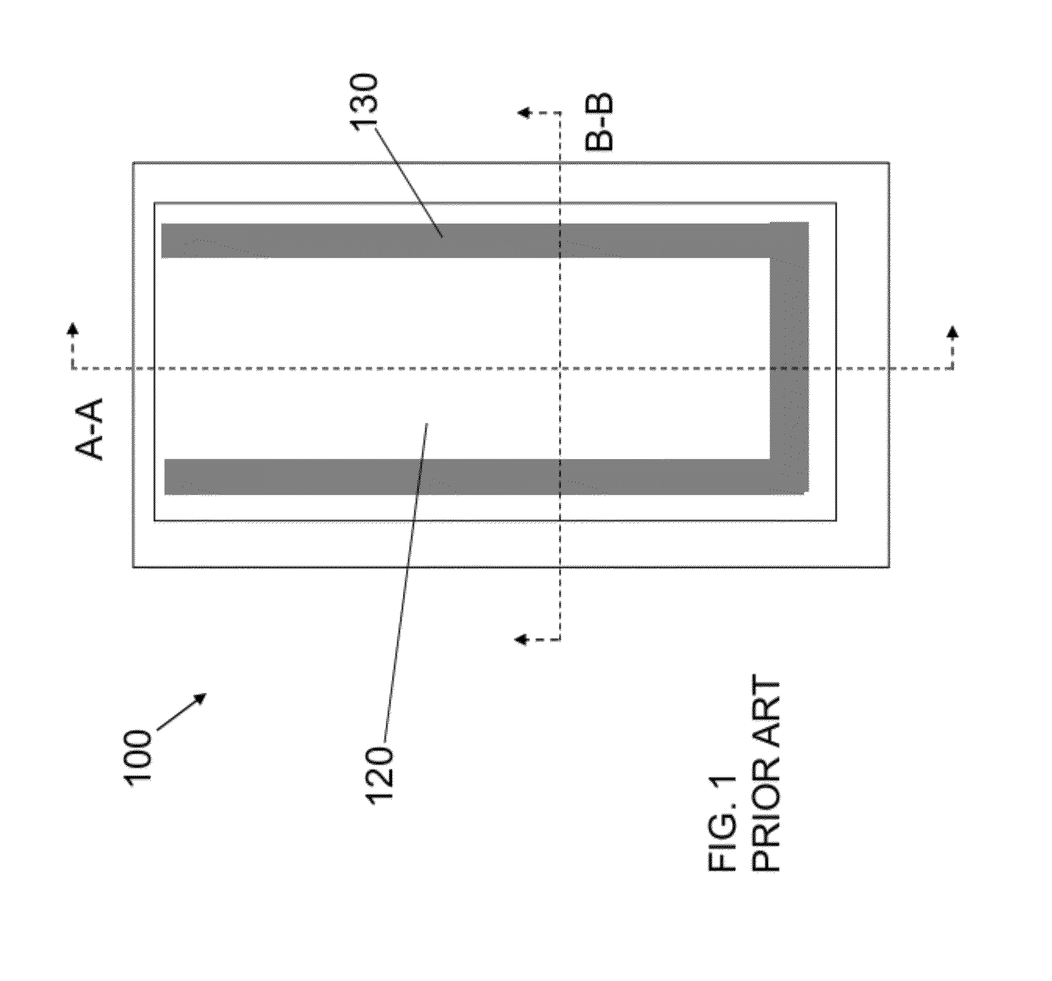
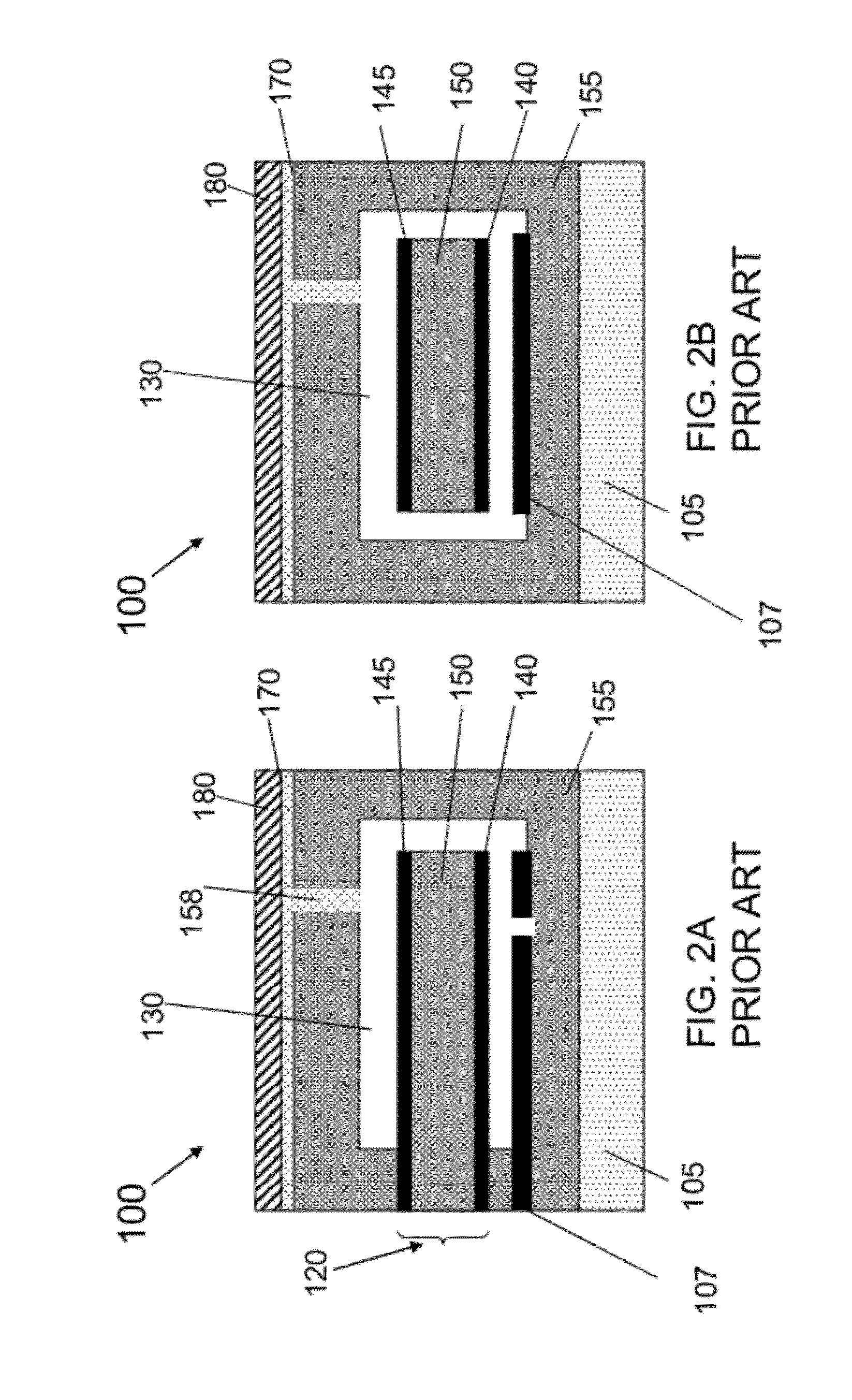
[0023]As used herein, the term “deposition” or “depositing” may include any now known or later developed techniques appropriate for the material to be deposited including but are not limited to, for example: chemical vapor deposition (CVD), low-pressure CVD (LPCVD), plasma-enhanced CVD (PECVD), sub-atmosphere CVD (SACVD), atmospheric pressure CVD (APCVD), high density plasma CVD (HDPCVD), rapid thermal CVD (RTCVD), ultra-high vacuum CVD (UHVCVD), limited reaction processing CVD (LRPCVD), metalorganic CVD (MOCVD), sputtering deposition, ion beam deposition, electron beam deposition, laser assisted deposition, thermal oxidation, thermal nitridation, spin-on methods, physical vapor deposition (PVD), atomic layer deposition (ALD), chemical oxidation, molecular beam epitaxy (MBE), plating, or evaporation. The figures shown herein are not drawn to scale and, in particular, many are drawn exaggerating the y axis or compressing the x axis. In one exemplary embodiment, the beam thickness, ga...


PUM


Abstract

In one embodiment, a semiconductor structure includes a beam positioned within a sealed cavity, the beam including: an upper insulator layer including one or more layers; and a lower insulator layer including one or more layers, wherein a composite stress of the upper insulator layer is different than a composite stress of the lower insulator layer, such that the beam bends.

Description

CROSS-REFERENCE TO RELATED APPLICATIONS[0001]This application is related in some aspects to commonly owned and co-pending patent application number (to be provided), entitled “METHOD OF FORMING OXIDE MEMS BEAM”, assigned attorney docket number BUR9201000154US1, filed Nov. 29, 2010, the entire contents of which are herein incorporated by reference.BACKGROUND[0002]1. Technical Field[0003]The disclosure relates generally to micro electro-mechanical systems (MEMS), and more particularly, to an oxide MEMS beam including a stress gradient.[0004]2. Background Art[0005]Micro Electro Mechanical Systems (MEMS) switches are fabricated such that there is a movable beam electrode which, when electrostatically actuated, makes contact to a second electrode. The second electrode is usually fixed to a surface under or over the movable beam electrode. The movable beam electrode, which can be, for example, a cantilever or bridge beam, is fabricated such that it is surrounded by a sacrificial material,...

Claims


Application Information

Patent Timeline
Patent Type & Authority Applications(United States)
IPC IPC(8): H01L29/84
CPCB81B3/0072B81B2203/0118H01G5/18H01G5/16B81C2201/0167
Inventor HASSELBACH, JOSEPH P.LESTAGE, KAREN L.STAMPER, ANTHONY K.
Owner IBM CORP
Why Eureka
Try Eureka