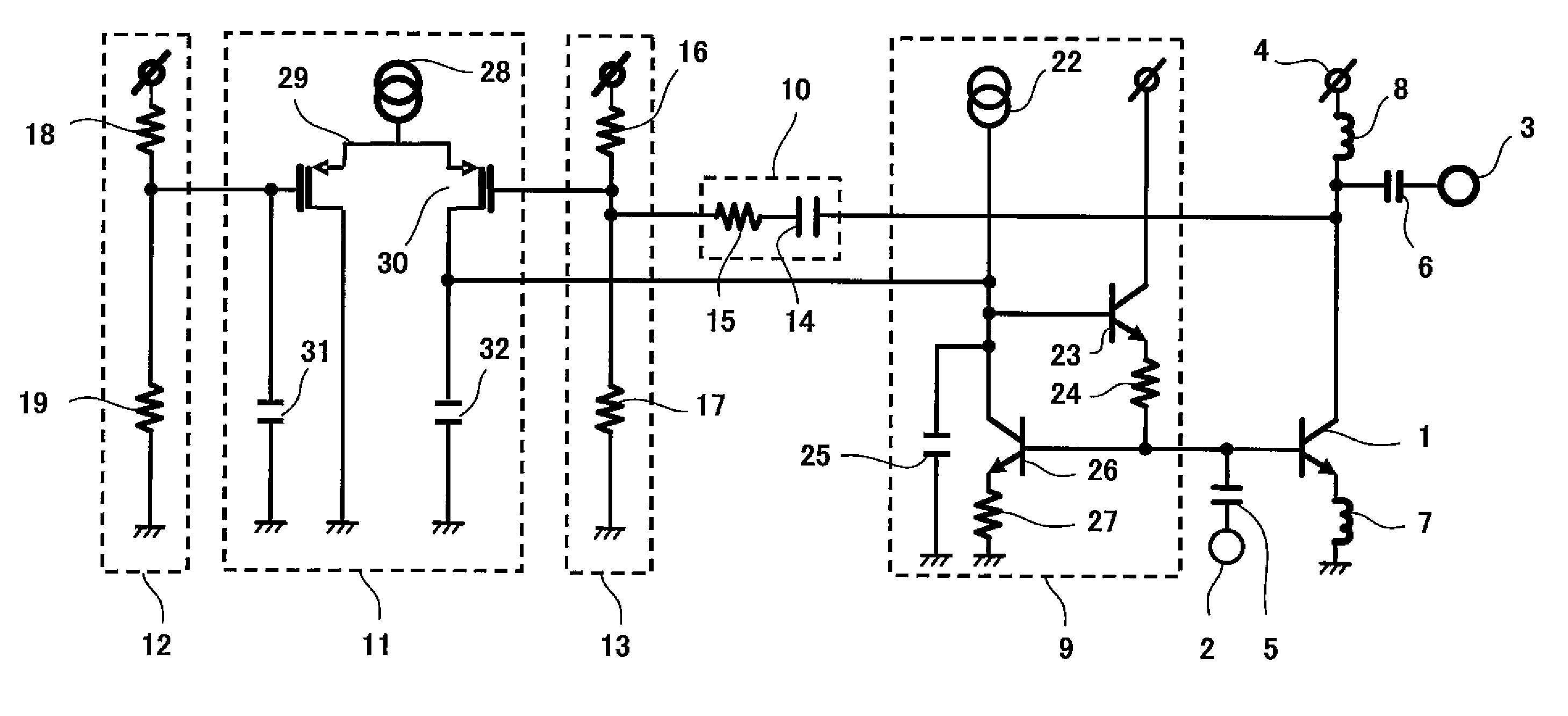
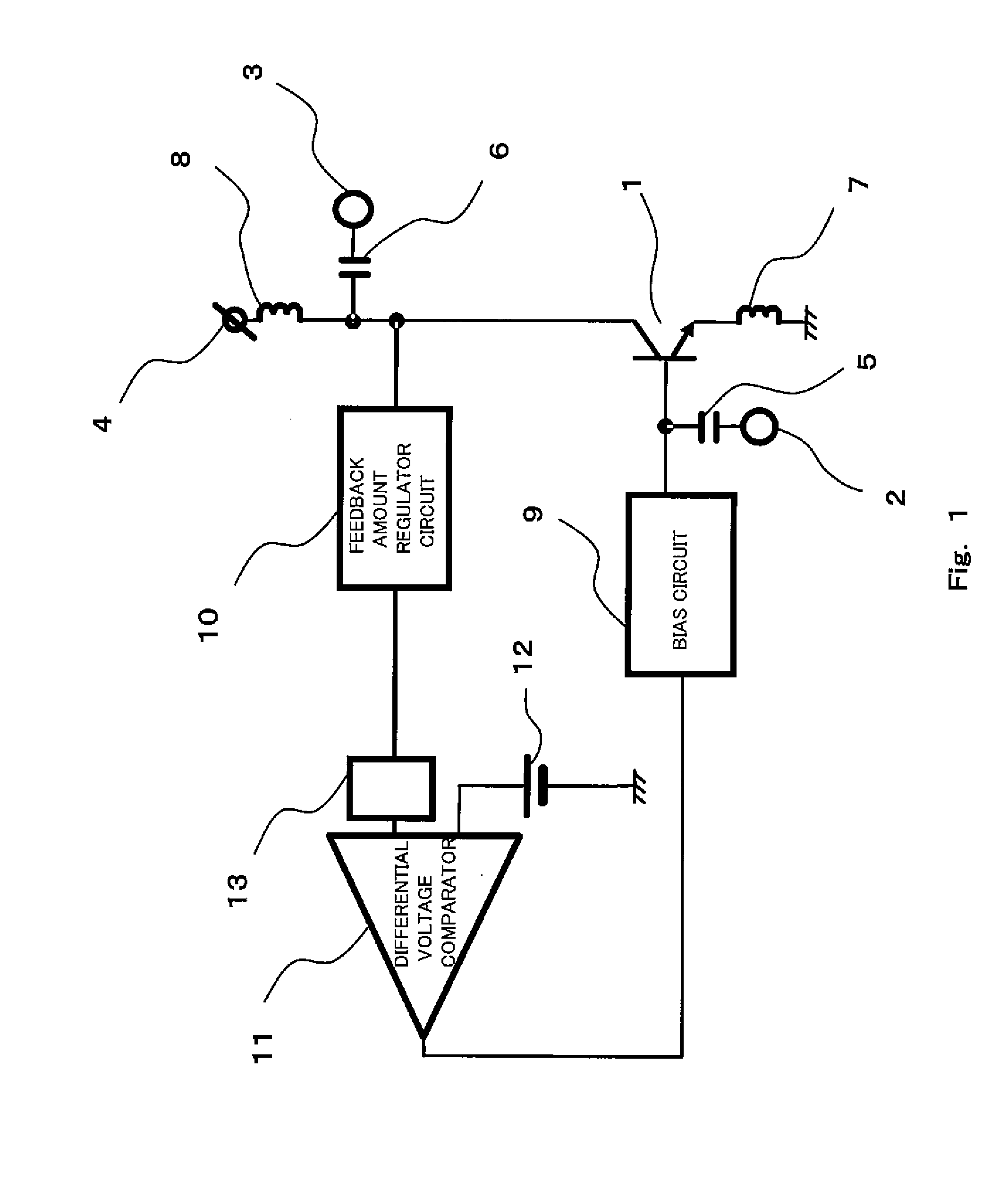
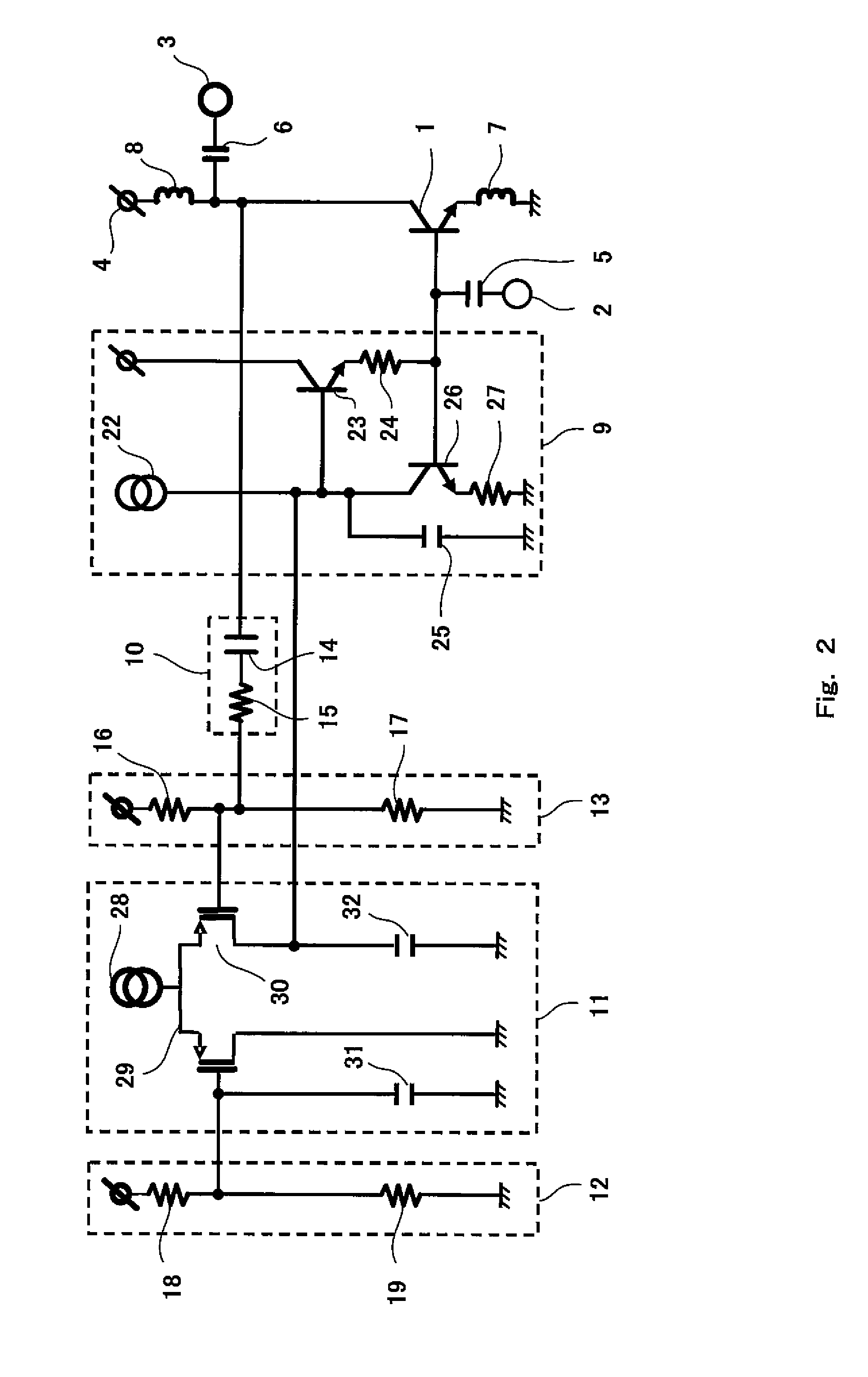
[0010]The present invention has been developed under the circumstances, and an object of the present invention is to reduce the degree to which a
gain of a transistor is suppressed by increasing a bias current fed to a transistor when a high-level disturbing wave signal which causes the gain of the transistor to be suppressed is input, in a case where a weak
electric field is input, in a low-noise amplifier. Another object of the present invention is to achieve the above
advantage stably, even when there is a variation in characteristics of elements in manufacturing or a change or variation in power supply voltages.
[0012]In accordance with this configuration, when a high-level disturbing wave signal which causes the gain of the transistor to be suppressed is input to the input terminal, in a case where a case a weak
electric field is input, in the low-noise amplifier, the degree to which the gain of the transistor is suppressed can be reduced effectively by increasing the bias current fed to the transistor. Also, when the high-level disturbing wave signal is not input, the bias current fed to the transistor is not increased, and as a result,
electric power consumption can be suppressed. In addition, by providing first and second input bias circuits for regulating two input biases (bias voltages) of the differential voltage comparator, the above
advantage is achieved stably even when there is a variation in the characteristics of elements in manufacturing, or a change or variation in power supply voltages.
[0014]In accordance with this configuration, it is possible to desirably and easily set the amplitude of the voltage applied from the feedback amount regulator circuit to the other input end of the differential voltage comparator, by impedance of the
resistor and the DC
cut capacitor. In addition, it is possible to prevent a DC component of the signal output from the transistor from being applied to the other input end of the differential voltage comparator, by using the DC
cut capacitor. Thus, the operation of the differential voltage comparator can be stabilized, and the level of the disturbing wave signal at which the bias current fed to the transistor begins to increase does not vary, even when the
power supply voltage supplied to the low-noise amplifier varies. As a result, it is possible to stably achieve an effect of reducing degree to which the gain of the transistor is suppressed.
[0016]In accordance with this configuration, the level of the disturbing wave signal at which the bias current of the transistor begins to increase can be set desirably and easily merely by regulating (adjusting) a resistance ratio between the plurality of resistors. Because of this, in addition, an influence of a variation in the power supply voltages and a variation in the elements in manufacturing can be lessened, and the effect of reducing the degree to which the gain of the transistor is suppressed can be achieved stably.
[0018]In accordance with this configuration, when the level of the disturbing wave signal increases, an increase amount of the bias current fed to the transistor can be desirably and easily set by regulating (adjusting) a mirror ratio of the
current mirror circuits. An
electric potential at a connection point where the bias circuit is connected to the
current mirror circuit, rises with an increase in the bias current fed to the transistor. Therefore, during low-voltage driving, a changing magnitude of the bias current fed to the transistor is restricted by an amount corresponding to a drop (decrease) amount of the
power supply voltage. However, a drop (decrease) amount of the voltage in the
current mirror circuit corresponds to only a drain-source voltage of the
MOSFET constituting the current mirror circuit. Therefore, even during low-voltage driving, a changing magnitude of the bias current fed to the transistor can be ensured.
[0019]In accordance with the low-noise amplifier of the present invention, when a high-level disturbing wave signal which causes the gain of the transistor to be suppressed is input to the input terminal, in a case a weak
electric field is input, the degree to which the gain of the transistor is suppressed can be reduced effectively by increasing the bias current fed to the transistor. Also, when the high-level disturbing wave signal is not input, the bias current fed to the transistor is not increased, and as a result,
electric power consumption can be suppressed. In addition, such an
advantage is achieved stably even when there is a variation in the characteristics of the elements in manufacturing, or a change or variation in the power supply voltages.

