Solar cell

a solar cell and cell technology, applied in the field of solar cells, can solve the problems of insufficient energy conversion efficiency and approaching the theoretical limit of shockle-quisser, and achieve the effect of further heightened incident photon-to-current conversion efficiency

Inactive Publication Date: 2012-06-28
THE UNIV OF TOKYO +1
View PDF2 Cites 14 Cited by
  • Summary
  • Abstract
  • Description
  • Claims
  • Application Information

AI Technical Summary

Benefits of technology

[0015]Such optical excitation via the intermediate energy level enables the electrons to be generated in the conduction band of the barrier layer and holes to be generated in the valence band of the barrier layer and them to be optically converted. As a result, a photovoltaic power can be generated. Since such photoelectric conversion can utilize incident light with a longer wavelength, incident photon-to-current conversion eff

Problems solved by technology

However, energy conversion efficiency is approaching a theoretical limit of Shockle-Quisser (hereinafter referred to as SQ theoretical

Method used


Image

  • Solar cell
  • Solar cell
  • Solar cell

Examples


experiment 1

Simulation Experiment 1

[Experiment 1]

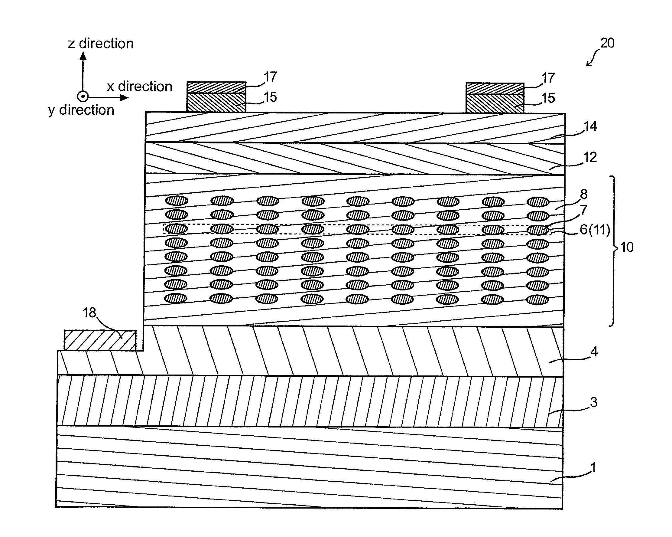
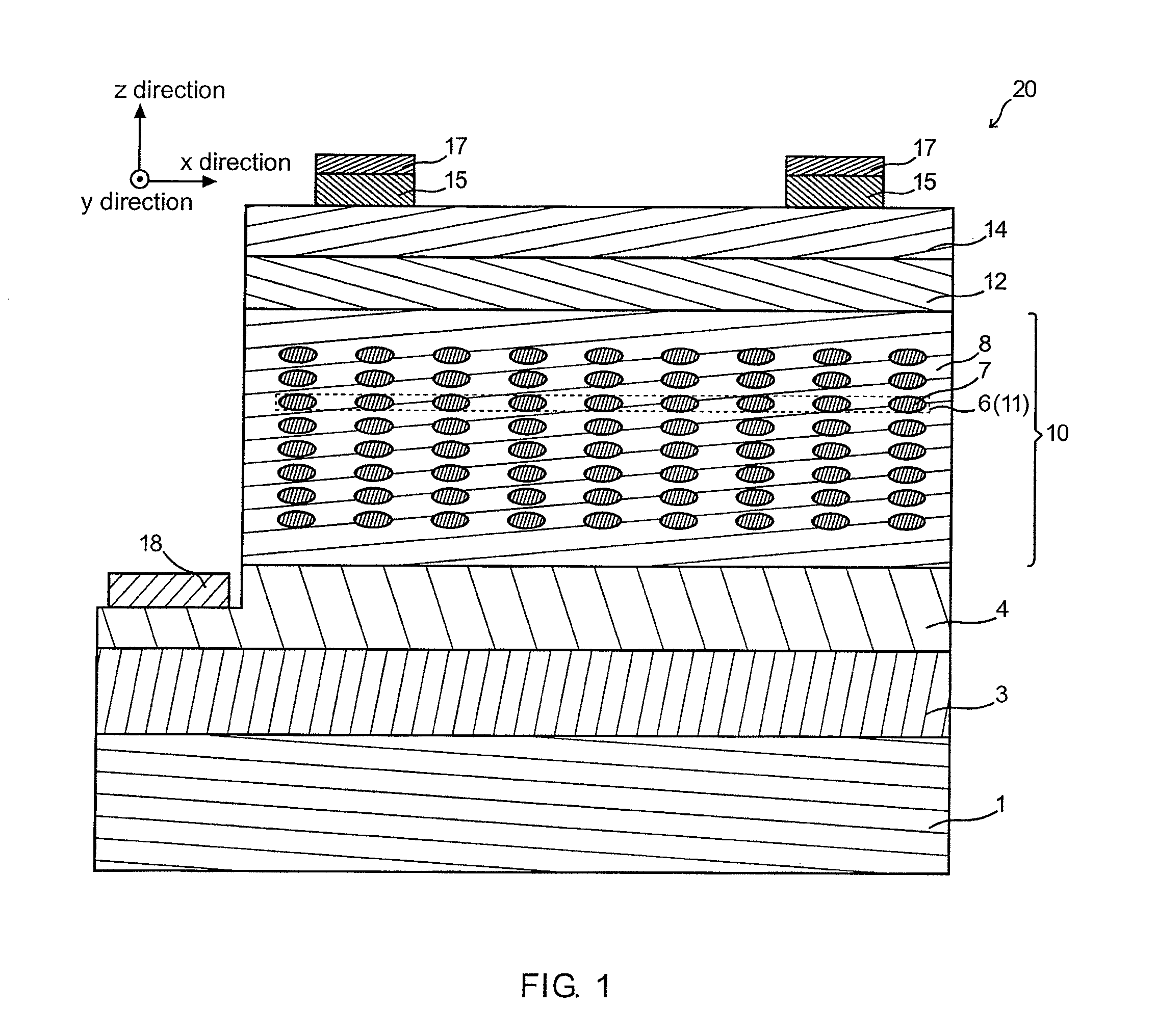
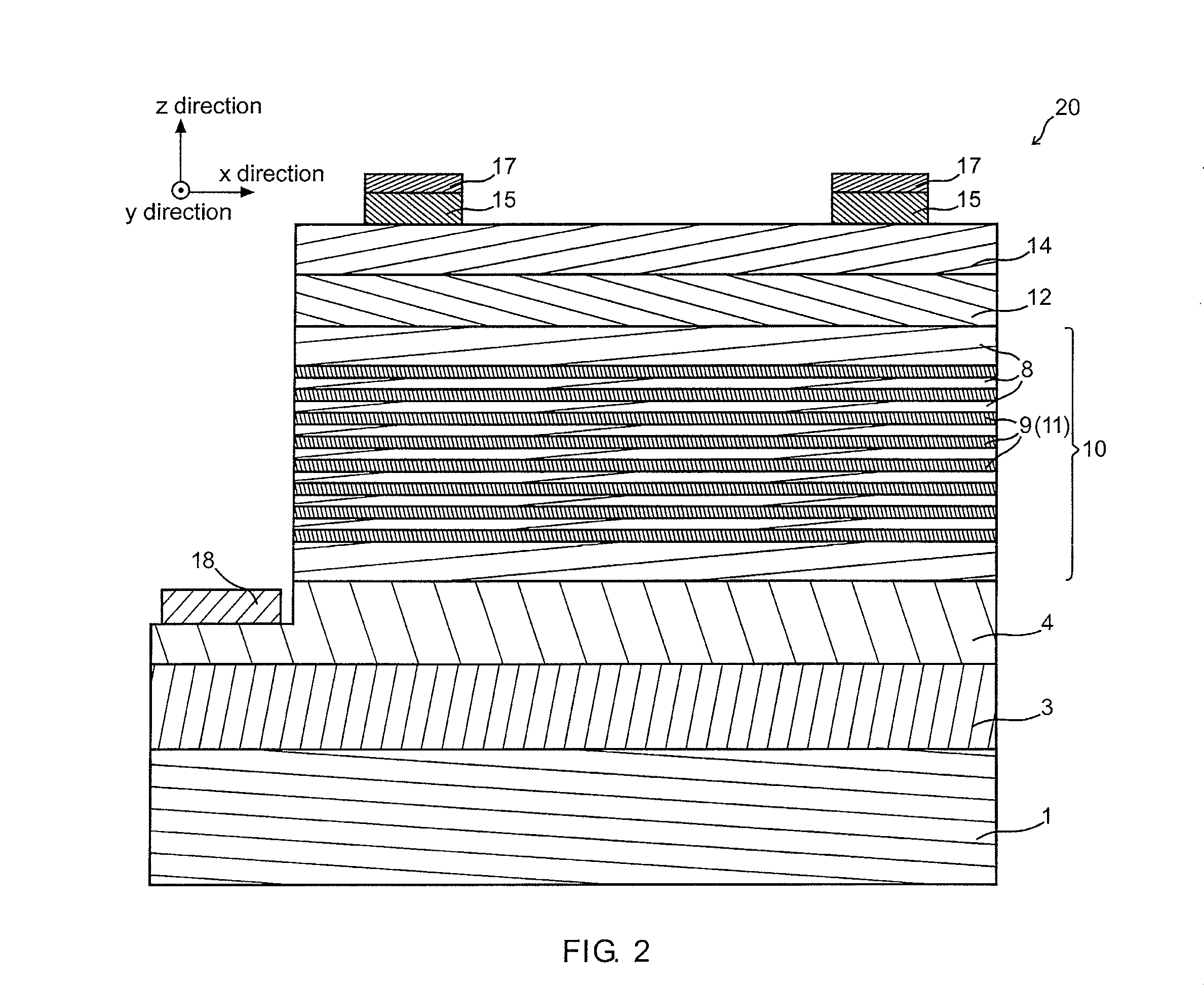
[0147]A simulation experiment was carried out by using a detailed balance model, so that the energy conversion efficiency was calculated. In order to describe this calculating method, band diagrams are shown in FIGS. 3 and 4. In this simulation experiment, the quantum dot layer was used as the quantum layer.

[0148]FIG. 3 is a band diagram of a superlattice semiconductor layer, which has four intermediate energy levels (the intermediate bands) and is included in the solar cell (6-levels intermediate-band solar cell) according to one embodiment of the present invention, and is an explanatory diagram describing a positional relationship of six levels.

[0149]FIG. 4 is a band diagram of the superlattice semiconductor layer, which has the four intermediate energy levels and is included in the solar cell (6-levels intermediate-band solar cell) according to one embodiment of the present invention, and is an explanatory diagram describing a relationship bet...

experiment 2

Simulation Experiment 2

[0214]A simulation experiment is further conducted on the superlattice semiconductor layer, which has the energy levels and is included in the solar cell (the 4 to 6-levels intermediate-band solar cell: referred also as a multi-level intermediate-band solar cell) shown in the experiments 1 to 3, with an attention being paid to a specific structure.

[0215]The Schrodinger equation is solved by using MATLAB software, and a band structure is calculated. In this simulation experiment, as a structure that can realize the multi-level intermediate-band solar cell, an attention is paid to “a structure where the valence band offset is 0” and “a structure where the valence band offset is not 0”. A shape of the quantum dot is considered as a cube, and a size of three sides are (x nm, y nm, z nm).

experiment 4

[Experiment 4]

[0216]A band structure is calculated in the intermediate-band solar cell having a structure where the valence band offset is 0.

[0217]In the superlattice semiconductor layer having the superlattice structure where the barrier layers made of AlSb and the quantum dot layers made of the quantum dots of InAs1-xSbx are stacked repeatedly, a difference between the energy level at the top of the valence band in the barrier layer and the energy level at the top of the valence band in the material (bulk) composing the quantum dots can be set to 0, and the valence band offset can be 0 (the valence band offset is such that a difference in the energy level of the top of the valence band between InAsxSb1-x and AlSb is 0). Since the electrons of InAs1-xSbx are quantum confined in AlSb at a point Γ, the band structures of InAs1-xSbx and AlSb at the point Γ are considered. The following calculation is made under a condition that x=0.3 according to the Vegard's law. The band gap of AlSb...


PUM


Abstract

A solar cell of the present invention comprises a p-type semiconductor layer, an n-type semiconductor layer and a superlattice semiconductor layer sandwiched between the p-type semiconductor layer and the n-type semiconductor layer, wherein the superlattice semiconductor layer has a superlattice structure in which barrier layers and quantum layers are stacked alternately and repeatedly, and has two or more intermediate energy levels where electrons optically excited from a valence band of the quantum layers or the barrier layers stay for a constant time, the intermediate energy levels being located between a top of the valence band of the barrier layers and a bottom of a conduction band of the barrier layers, and can achieve a high incident photon-to-current conversion efficiency.

Description

CROSS-REFERENCE TO RELATED APPLICATION[0001]This application is related to Japanese Patent Application Nos. 2010-286397 filed on Dec. 22, 2010 and 2011-056951 filed on Mar. 15, 2011, whose priorities are claimed under 35 USC §119, and the disclosures of which are incorporated by reference in its entirety.BACKGROUND OF THE INVENTION[0002]1. Field of the Invention[0003]The present invention relates to a solar cell having a superlattice structure.[0004]2. Description of the Related Art[0005]In recent years, an attention is paid to photovoltaic elements as clean energy sources that do not emit CO2, and thus they are being widely used. In such photovoltaic elements, currently the most popular photovoltaic elements are unijunction solar cells using silicon. However, energy conversion efficiency is approaching a theoretical limit of Shockle-Quisser (hereinafter referred to as SQ theoretical limit). For this reason, third-generation solar cells that exceed the SQ theoretical limit are being...

Claims


Application Information

Patent Timeline
IPC IPC(8): H01L31/072
CPCB82Y20/00H01L31/03046Y02E10/544H01L31/035236H01L31/035218
Inventor ARAKAWA, YASUHIKONOZAWA, TOMOHIROIZUMI, MAKOTO
Owner THE UNIV OF TOKYO
Why Eureka
Try Eureka