Semiconductor device and manufacturing method thereof

a technology of semiconductors and semiconductors, applied in the direction of solid-state devices, transistors, climate sustainability, etc., can solve the problems of increasing the cost per storage capacity, short data holding period, and difficulty in sufficiently reducing power consumption

Active Publication Date: 2012-06-28
SEMICON ENERGY LAB CO LTD
View PDF8 Cites 63 Cited by
  • Summary
  • Abstract
  • Description
  • Claims
  • Application Information

AI Technical Summary

Benefits of technology

[0012]In view of the above problem, it is an object of an embodiment of the present invention to provide a novel semiconductor device which can hold data even when power is not supplied in a data storing time, and which does not have a limitation on the number of writing operations.
[0013]In the present invention, a semiconductor device is formed using a material which allows a sufficient reduction in off-state current of a transistor; for example, an oxide semiconductor material, which is a wide-gap semiconductor, is used. The use of the semiconductor material which allows a sufficient reduction in off-state current of a transistor makes it possible to hold data for a long period. Further, an oxide semiconductor material has high permittivity; thus, the use of the oxide semiconductor material for a dielectric of a capacitor enables an increase in capacitance per unit area.
[0029]The off-state current of a transistor including an oxide semiconductor is extremely low and thus stored data can be stored for an extremely long time by using the transistor. In other words, power consumption can be reduced because refresh operation becomes unnecessary or the frequency of refresh operation can be extremely low. Moreover, stored data can be held for a long time even when power is not supplied, but note that potentials are preferably fixed.
[0030]An oxide semiconductor material has high permittivity; thus, the use of the oxide semiconductor material for a dielectric of a capacitor enables an increase in capacitance per unit area. Consequently, the area of the capacitor can be reduced, so that high integration is possible and a semiconductor device can be miniaturized. In addition, the frequency of refresh operations can be further reduced and thus power consumption can be further reduced.
[0031]Further, a semiconductor device according to one embodiment of the present invention does not need high voltage for data writing and there is no problem of deterioration of elements. For example, unlike a conventional non-volatile memory, it is not necessary to inject and extract electrons into and from a floating gate and thus a problem such as deterioration of a gate insulating layer does not occur at all. In other words, the semiconductor device according to one embodiment of the present invention does not have a limit on the number of writing times which is a problem in a conventional nonvolatile memory, and reliability thereof is drastically improved. Furthermore, data is written depending on the on state and the off state of the transistor, whereby high-speed operation can be easily realized. In addition, there is no need of operation for erasing data.
[0032]Further, a transistor containing a material other than an oxide semiconductor can operate at sufficiently high speed; thus, by using the transistor, a variety of circuits (e.g., a logic circuit or a driver circuit) in which high-speed operation is needed can be favorably realized.

Problems solved by technology

Moreover, since leakage current (off-state current) flows between a source and a drain of a transistor included in a memory element when the transistor is in an off state, charge flows into or out even if the transistor is not selected, which makes a data holding period short.
For that reason, another writing operation (refresh operation) is necessary at predetermined intervals, and it is difficult to sufficiently reduce power consumption.
Furthermore, since stored data is lost when power supply stops, an additional storage device using a magnetic material or an optical material is needed in order to hold the data for a long time.
However, cost per storage capacity is increased because a circuit such as a flip-flop is used.
Moreover, as in a DRAM, stored data in an SRAM is lost when power supply stops.
However, a gate insulating layer included in a storage element deteriorates by tunneling current generated in writing, so that the storage element stops its function after a predetermined number of writing operations.
However, a complicated peripheral circuit is needed to realize this method.
Moreover, employing such a method does not solve the fundamental problem of lifetime.
In other words, a flash memory is not suitable for applications in which data is frequently rewritten.
Further, it takes a relatively long time to hold or remove electric charge, and it is not easy to perform writing and erasing at higher speed.

Method used


Image

  • Semiconductor device and manufacturing method thereof
  • Semiconductor device and manufacturing method thereof
  • Semiconductor device and manufacturing method thereof

Examples


embodiment 1

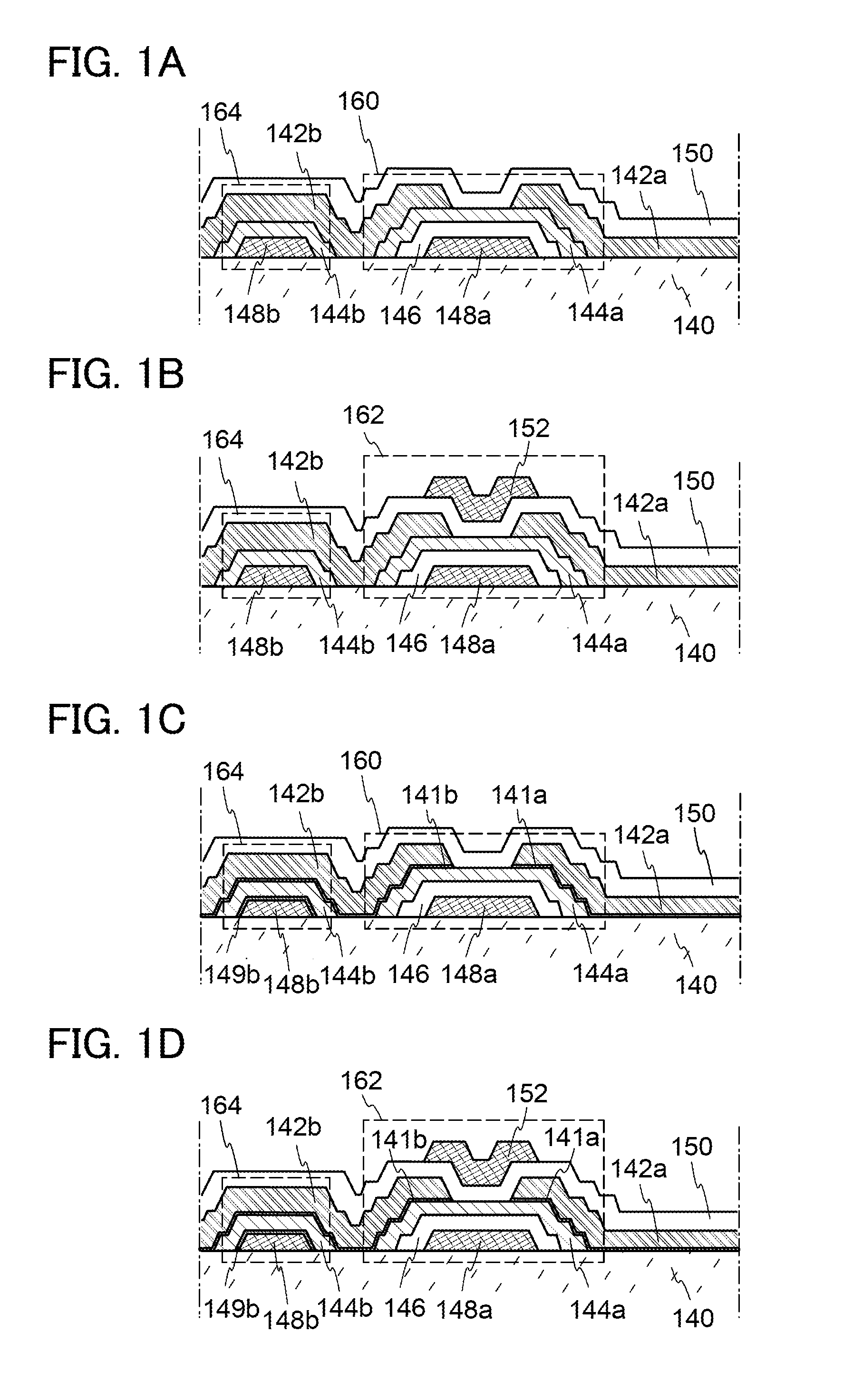
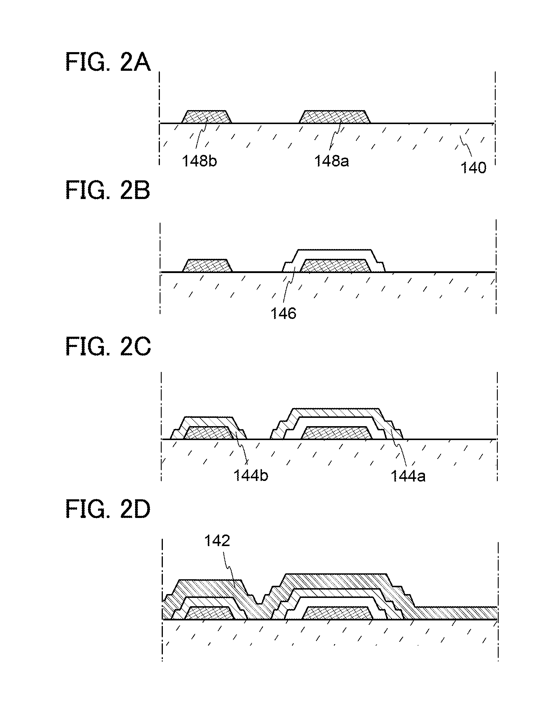
[0057]In this embodiment, a structure and a manufacturing method of a semiconductor device according to one embodiment of the present invention will be described with reference to FIGS. 1A to 1D, FIGS. 2A to 2D, and FIGS. 3A to 3C.

[0058]FIGS. 1A to 1D are structure examples of semiconductor devices. FIGS. 1A to 1D illustrate cross sections of the semiconductor devices. The semiconductor devices shown in FIGS. 1A and 1C each include a transistor 160 whose channel formation region includes an oxide semiconductor and a capacitor 164 whose dielectric includes an oxide semiconductor. The semiconductor devices shown in FIGS. 1B and 1D each include a transistor 162 whose channel formation region includes an oxide semiconductor and the capacitor 164 whose dielectric includes an oxide semiconductor.

[0059]Although all the transistors are described as n-channel transistors here, it is needless to say that p-channel transistors can be used. Since the technical nature of the disclosed invention ...

embodiment 2

[0159]In this embodiment, a structure and a method of manufacturing a semiconductor device, which are different from those of Embodiment 1, will be described with reference to FIGS. 4A and 4B, FIGS. 5A to 5D, FIGS. 6A to 6C, FIGS. 7A and 7B, and FIGS. 8A to 8D.

[0160]FIGS. 4A and 4B are structural examples of a semiconductor device. FIGS. 4A and 4B illustrate cross sections of the semiconductor device. The semiconductor devices shown in FIGS. 4A and 4B each include the transistor 160 whose channel formation region includes an oxide semiconductor and the capacitor 164 whose dielectric includes an oxide semiconductor.

[0161]The transistor 160 in FIG. 4A includes the source or drain electrode 142b and the drain or source electrode 142a which are provided over the insulating layer 140; the first oxide semiconductor layer 144a over and electrically connected to the source or drain electrode 142b and the drain or source electrode 142a; the gate insulating layer 146 covering the first oxide ...

embodiment 3

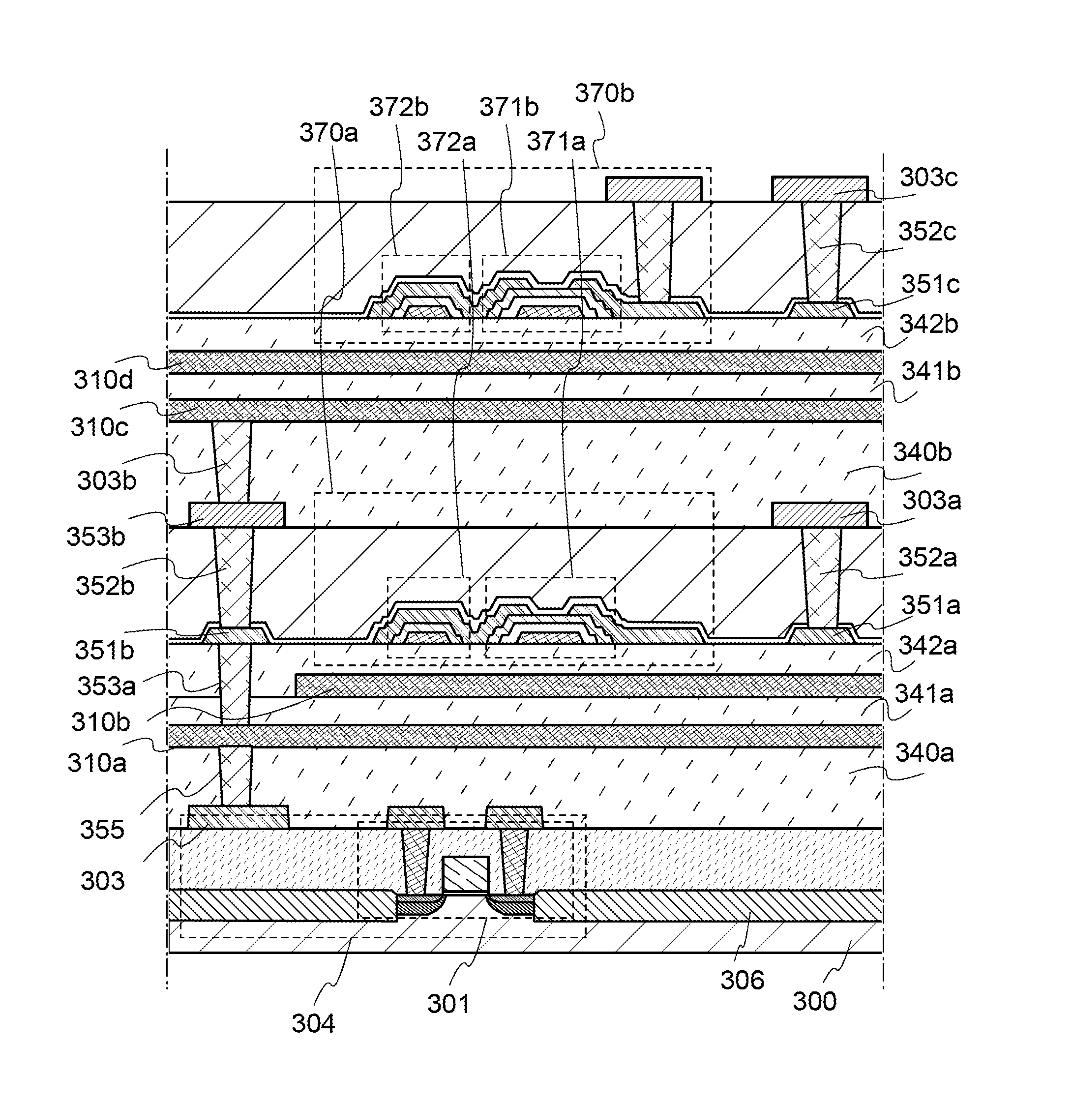
[0229]In this embodiment, an example of a memory cell 170 including the semiconductor devices in Embodiment 1 and Embodiment 2 will be shown with reference to FIGS. 9A to 9C.

[0230]FIG. 9A is a cross-sectional view of the memory cell 170. FIG. 9B is a top-view of the memory cell 170. FIG. 9C is a circuit diagram of the memory cell 170.

[0231]FIGS. 9A and 9B corresponds to the semiconductor device of FIG. 1A; however, this embodiment is not limited thereto. Any of the semiconductor devices of FIGS. 1A to 1D, FIGS. 3A to 3C, and FIGS. 4A and 4B can be used, and alternatively, another semiconductor device with a function similar to the structure of the semiconductor devices can be used.

[0232]The memory cell 170 of FIGS. 9A to 9C includes the transistor 160 and the capacitor 164.

[0233]In the memory cell 170 of FIG. 9A, the drain or source electrode 142a of the transistor 160 is electrically connected to a wiring 156 through an opening in the insulating layer 150 and an insulating layer 15...


PUM

PropertyMeasurementUnit
energy gap Egaaaaaaaaaa
work functionaaaaaaaaaa

Abstract

An object is to provide a novel semiconductor device which can store data even when power is not supplied in a data storing time and which does not have a limitation on the number of writing operations. The semiconductor device includes a transistor and a capacitor. The transistor includes a first oxide semiconductor layer, a source electrode and a drain electrode which are in contact with the first oxide semiconductor layer, a gate electrode overlapping with the first oxide semiconductor layer, and a gate insulating layer between the first oxide semiconductor layer and the gate electrode. The capacitor includes the source electrode or the drain electrode, a second oxide semiconductor layer in contact with the source electrode or the drain electrode, and a capacitor electrode in contact with the second oxide semiconductor layer.

Description

BACKGROUND OF THE INVENTION[0001]1. Field of the Invention[0002]The present invention relates to a semiconductor device using a semiconductor element and a method for driving the semiconductor device.[0003]2. Description of the Related Art[0004]Storage devices using semiconductor elements are broadly classified into two categories: a volatile device that loses stored data when power supply stops, and a non-volatile device that retains stored data even when power is not supplied.[0005]A typical example of a volatile storage device is a DRAM (dynamic random access memory). A DRAM stores data in such a manner that a transistor included in a storage element is selected and charge is stored in a capacitor.[0006]When data is read from a DRAM, electric charge in a capacitor is lost on the above principle; thus, another writing operation is necessary every time data is read. Moreover, since leakage current (off-state current) flows between a source and a drain of a transistor included in a ...

Claims


Application Information

Patent Timeline
Patent Type & Authority Applications(United States)
IPC IPC(8): H01L29/786H01L29/02
CPCH01L27/1225H01L27/1255C04B2235/3286C04B35/58C04B2235/3284H01L29/78648Y02D10/00H01L21/02172H01L21/02554H01L29/78606H01L29/78618H01L29/7869
Inventor YAMAZAKI, SHUNPEI
Owner SEMICON ENERGY LAB CO LTD
Why Eureka
Try Eureka