Integrated organic light-emitting device, method for producing organic light-emitting device and organic light-emitting device produced by the method

a technology of organic light and light, which is applied in the manufacture of electric discharge tubes/lamps, tube/lamp factory adjustment, discharge tubes luminescnet screens, etc., can solve the problems of reducing luminance efficiency and expanded brightness distribution, accelerating deterioration of organic thin films, and affecting the quality of organic light, so as to inhibit the expansion of brightness distribution and heat generated in power distribution, the effect of high resistan

Active Publication Date: 2012-06-28
KANEKA CORP
View PDF4 Cites 14 Cited by
  • Summary
  • Abstract
  • Description
  • Claims
  • Application Information

AI Technical Summary

Benefits of technology

[0041]This invention can provide a highly reliable high-performance organic EL device of a large area, that considerably inhibits expanded brightness distribution and heat generated in power distribution to high-brightness organic EL elements using a light-transmissive conductive material, which normally has a high resistance, for an electrode.

Problems solved by technology

It is known that this increase in current density normally generates heat, resulting in acceleration of deterioration of an organic thin film.
The higher resistance causes heat generation during power distribution, further resulting in many problems such as reduced luminance efficiency and expanded brightness distribution, in addition to the deterioration described above.
These problems are especially severe in application of surface-emitting organic EL devices to large-area illumination.
This technique is quite effective for a certain level of area enlargement, but has a problem in that the lamination involves an increased number of man-hours and materials, and further, too much lamination leads to a reduced brightness or luminance efficiency due to absorption of light by the resulting laminated body.
Basically, this technique is characterized in that it obtains a high brightness by an equivalent driving current, but because it does not reduce an absolute value of driving current density, it is limited as a means to enlarge the area.
This method may achieve the desired purpose to some extent, but is mostly premised on a mask process, resulting in a limitation in area enlargement and problems of complicated procedures and greater loss in the effective area.

Method used


Image

  • Integrated organic light-emitting device, method for producing organic light-emitting device and organic light-emitting device produced by the method
  • Integrated organic light-emitting device, method for producing organic light-emitting device and organic light-emitting device produced by the method
  • Integrated organic light-emitting device, method for producing organic light-emitting device and organic light-emitting device produced by the method

Examples


example 1

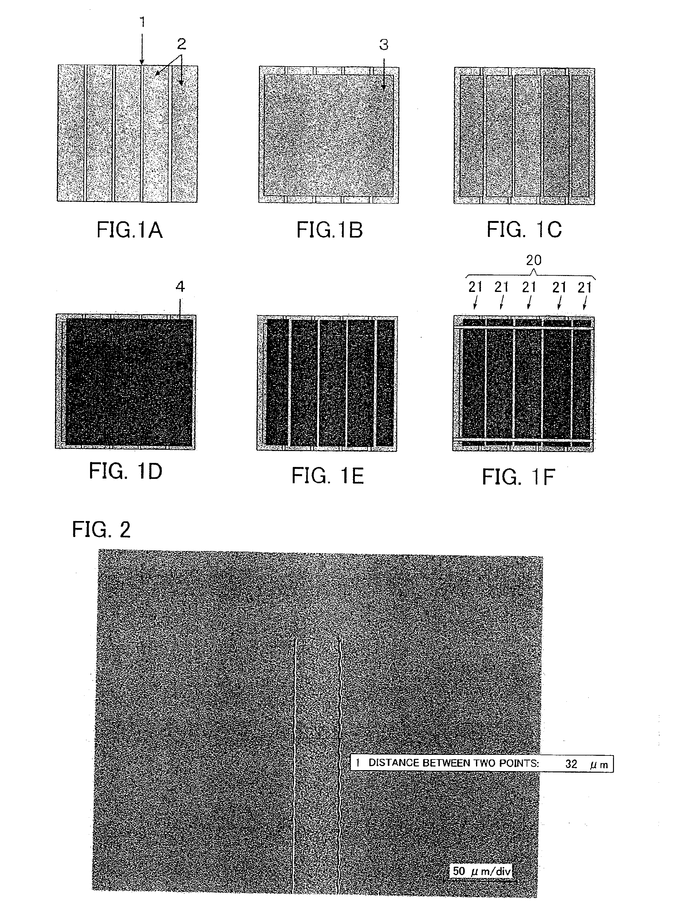
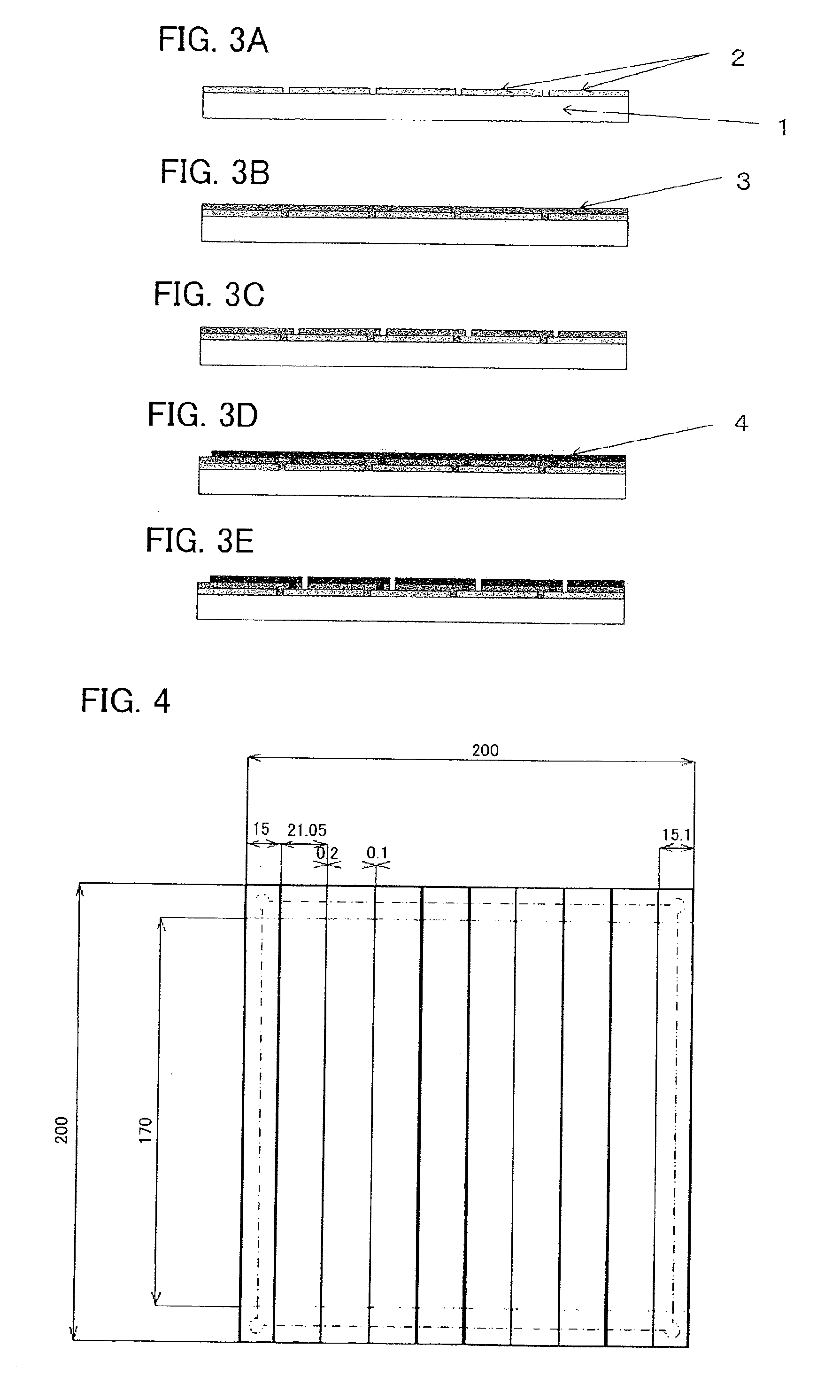
[0201]The light-transmissive substrate employed an alkali-free glass having a thickness of 0.7 mm and coated with an indium-doped tin oxide (ITO) film of 150 nm average film thickness on the entire surface. The substrate (200 mm×200 mm) was placed on an XY stage with the ITO film facing upward. A laser beam was applied from above using a light source of a fundamental harmonic of a YAG laser, so as to remove a part of the ITO film as shown in FIG. 1A while minimizing the possibility of damaging the glass. This step formed the first-electrode-layer dividing grooves 110 on the conductive electrode layer 102 by executing the first laser scribing step. The laser beam had an oscillation frequency of 15 kHz, an output power of 14 W, a beam diameter of about 25 μm, and a processing speed of 50 mm / second. FIG. 2 shows an enlarged planar photo of a laser-processed portion of the glass substrate with the patterned ITO film.

[0202]The resulting substrate was washed with a neutral detergent and h...

example 2

[0215]The substrate employed an alkali-free glass (200 mm×200 mm) having a thickness of 0.7 mm and coated with an ITO film of 150 nm average film thickness. The ITO film had undergone chemical etching into a form shown in FIG. 1A, and had an average etching width of 50 μm. The resulting substrate was washed with a neutral detergent and heated at 150 degrees centigrade for 20 minutes so as to be dried. It was confirmed that resistance values between strip-like ITO portions each were in general 20 MΩ or more. Thereafter, the resulting substrate was placed in a vacuum evaporator, as a result an organic EL device was produced in the same method as in Example 1. The performance of the integrated organic EL device produced in this method was measured in the same manner as Example 1. Average brightnesses of the same portions as those of Example 1 are shown in Table 1.

[0216]This Example executed a chemical etching on the light-transmissive conductive layer for the patterning in Example 1. D...

example 3

[0217]An integrated organic EL device was produced by the same method as in Example 1. Two adjacent strip-like pieces were chosen from the second electrode layer of the device so as to be subjected to the following procedure. A voltage of 0.1 V was applied in between the pieces in a direction opposite to the elements and resistances therebetween were measured. The results are shown by white circles (o) on the far left in FIG. 9. Thereafter, the applied voltage was increased repeatedly by 0.1 V and the resistances were measured each time until the voltage reached 5 V. The results are shown by white circles (o) other than those on the far left in FIG. 9. Then, after the applied voltage was decreased to 0 V, the voltages were increased repeatedly by 0.1 V and the resistances were measured until reaching 5 V. The results are shown by black circles () in FIG. 9. The results support that application of a voltage above a certain level eliminates micro defects and reduces leakage current. ...


PUM


Abstract

In a device according to the present invention, a first conductive electrode layer being patterned and light transmissive is formed on a light-transmissive substrate and a laminated layer containing a plurality of organic-compound layers is formed so as to cover at least a part of the first electrode layer. The laminated layer is partly removed so that the first electrode layer is partly exposed. At least one layer containing a second conductive electrode layer is formed on the laminated layer and the exposed part of the first electrode layer. A part of the laminated layer and a part of the second electrode layer are simultaneously removed by application of a laser beam from a side of the substrate, so that a plurality of light-emitting sections are electrically connected in series on the substrate.

Description

TECHNICAL FIELD[0001]The present invention relates to a method for producing an organic light-emitting device containing an organic layer as a surface light source or an organic electroluminescent (EL) device used mainly for illumination.[0002]The present invention also relates to a configuration of an organic light-emitting device.BACKGROUND ART[0003]Organic EL elements used in organic EL devices are semiconductor elements that convert electrical energy into optical energy. Recently, research using organic EL elements has been conducted at an accelerated pace. In the field of illumination, this research has already started to clarify issues with putting organic EL devices into practical use. Improved materials, such as an organic material that may form an organic EL element, achieve dramatically lowered driving voltages and increased luminance efficiency. Also, in the display market, televisions using organic EL elements for display screens have come to market.[0004]An increase in ...

Claims


Application Information

Patent Timeline
Patent Type & Authority Applications(United States)
IPC IPC(8): H05B33/14H05B33/10
CPCH01L27/3204H05B33/28H05B33/10H01L51/5203H10K59/86H10K50/805H10K71/00
Inventor YAMAGISHI, HIDEONISHIKAWA, AKIRAAYUKAWA, SHIGERU
Owner KANEKA CORP
Why Eureka
Try Eureka