Lead frame for optical semiconductor device, method of producing the same, and optical semiconductor device

Inactive Publication Date: 2012-07-05
FURUKAWA ELECTRIC CO LTD +1
View PDF3 Cites 15 Cited by
  • Summary
  • Abstract
  • Description
  • Claims
  • Application Information

AI Technical Summary

Benefits of technology

[0016]In the lead frame of the present invention, by forming, as an outermost layer, the metal oxide layer, which is colorless and transparent or silver gray in color, it is possible to prevent sulfurization and oxidation of the layer composed of silver or a silver alloy (i.e. an inner layer of the metal oxide layer) from being occurred, thereby to prevent a decrease of reflectance. Further, since the silver layer is not formed on the outermost surface (namely, silver is not exposed to the outside), no photocatalytic effect is exhibited. Thus, an optical semiconductor device can be provided, which exhibits a corrosion resistance and the effects in non-decomposition of the gas passed through the resin after resin sealing, and which has a good reflection property in the long term. In the lead frame of the present invention, when the metal oxide layer as an outermost layer is colorless and transparent or silver gray in color, and when the thickness thereof is controlled to be thin as thin as 0.001 to 0.2 μm, the reflection property is obtained, which almost does not decrease due to the metal oxide layer, and which is equivalent to that of conventional silver or a silver alloy.
[0017]The method of producing a lead frame of the present invention comprises the steps of: forming the layer composed of silver or a silver alloy on the electrically-conductive substrate; forming the metal layer composed of a metal other than silver, on the surface of the layer composed of silver or a silver alloy; and subjecting the metal layer to the heat treatment under an atmosphere of an oxygen concentration of 1,000 ppm or more, at a temperature from 100° C. to a melting point of the metal other than silver, thereby to form the metal oxide layer composed of an oxide of the metal other than silver as the surface layer. If necessary, the method of producing a lead frame of the present invention may further comprise the step of: causing diffusion of a remaining metal, which is the metal of the metal layer and remains as not oxidized, into the layer composed of silver or a silver alloy, thereby to form a silver alloy layer composed of a solid solution of the remaining metal and silver. Thus, the lattice strain is gradually relaxed and the adhesion property is improved. When the metal layer for forming the metal oxide layer is formed, by preferably plating (including wet plating, as well as dry plating, such as vacuum deposition), a thin and fine oxide layer can be readily formed.
[0018]Further, in the optical semiconductor device of the present invention, the metal oxide layer is provided at a portion on which an optical semiconductor element of the lead frame for the optical semiconductor devices is at least mounted, and thus the reflectance property can be efficiently obtained at a low cost. As for anther portion on which no optical semiconductor element is mounted, the layer composed of silver or a silver alloy may be exposed to the surface. In this case, the metal oxide layer may be partially formed on the layer composed of silver or a silver alloy, and it may be formed by partial plating, such as stripe plating or spot plating. Production of the lead frame with the thus-partially-formed layer makes it possible to cut off the amount of metal to be used at a portion where the layer is unnecessary, and thus the resultant optical semiconductor device can be friendly to the environment and can achieve reduction of the production costs.
[0019]Other and further features and advantages of the invention will appear more fully from the following description, appropriately referring to the accompanying drawings.

Problems solved by technology

However, as in the technique described in Patent Literature 1, when a layer composed of silver or a silver alloy was simply formed on a lead frame, a sulfurization reaction of the silver surface occurred, due to a sulfur component remaining in a sealing resin, to blacken, resulting in a decrease in the reflectance, which was a problem.
Further, the adhesion property between silver and a resin is relatively poor.
As a result, a gap occurred between the sealing resin and the silver plane, and a moisture and salt content permeated into the silver plane from the gap, resulting in migration, which was also a problem.
As in the technique described in Patent Literature 2, when the heat treatment was performed at a temperature 200° C. or higher, silver or a silver alloy was oxidized by the affection of the remaining oxygen, and the reflectance was decreased as compared with the case where such a means was not performed, which was another problem.
This is because a dark-brown silver oxide was formed on the surface layer, by oxidization of the silver or silver alloy, thereby causing a decrease in the reflectance.
As a result, we found a problem that the circumference of the LED was blackened and the reflectance was decreased.

Method used


Image

  • Lead frame for optical semiconductor device, method of producing the same, and optical semiconductor device
  • Lead frame for optical semiconductor device, method of producing the same, and optical semiconductor device
  • Lead frame for optical semiconductor device, method of producing the same, and optical semiconductor device

Examples


examples

[0076]The present invention will be described in more detail based on examples given below, but the invention is not meant to be limited by these.

example no.1

Example No. 1

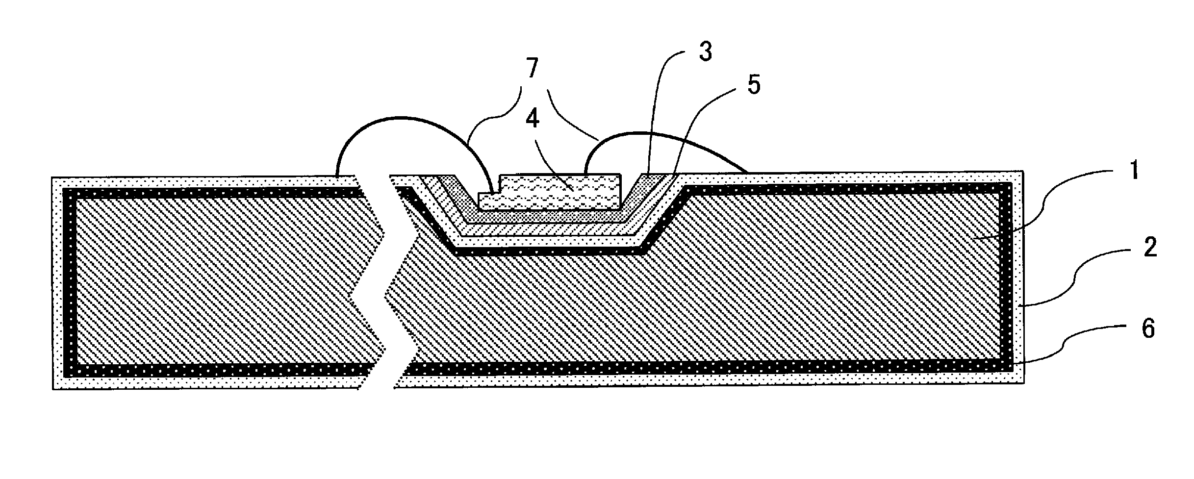
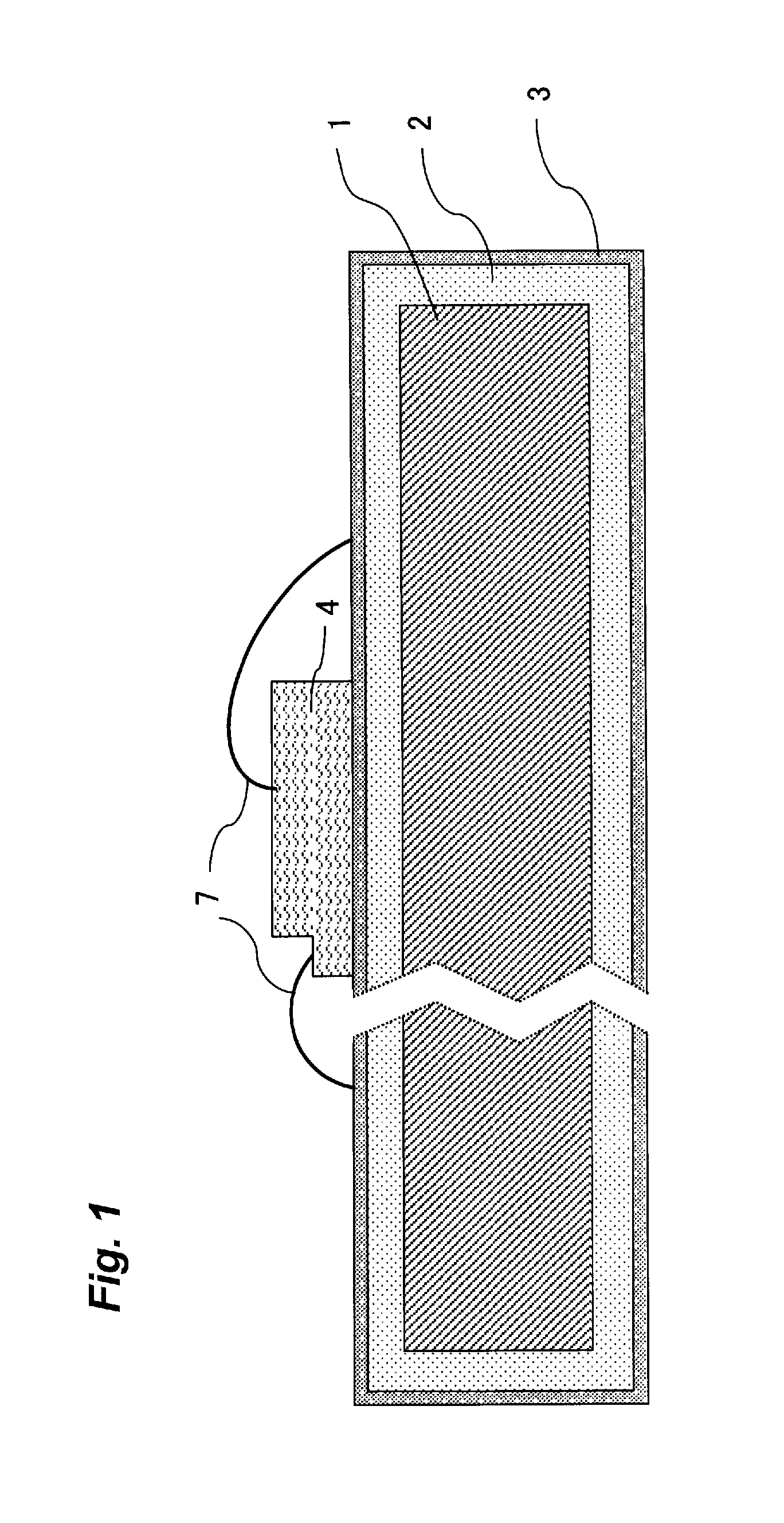
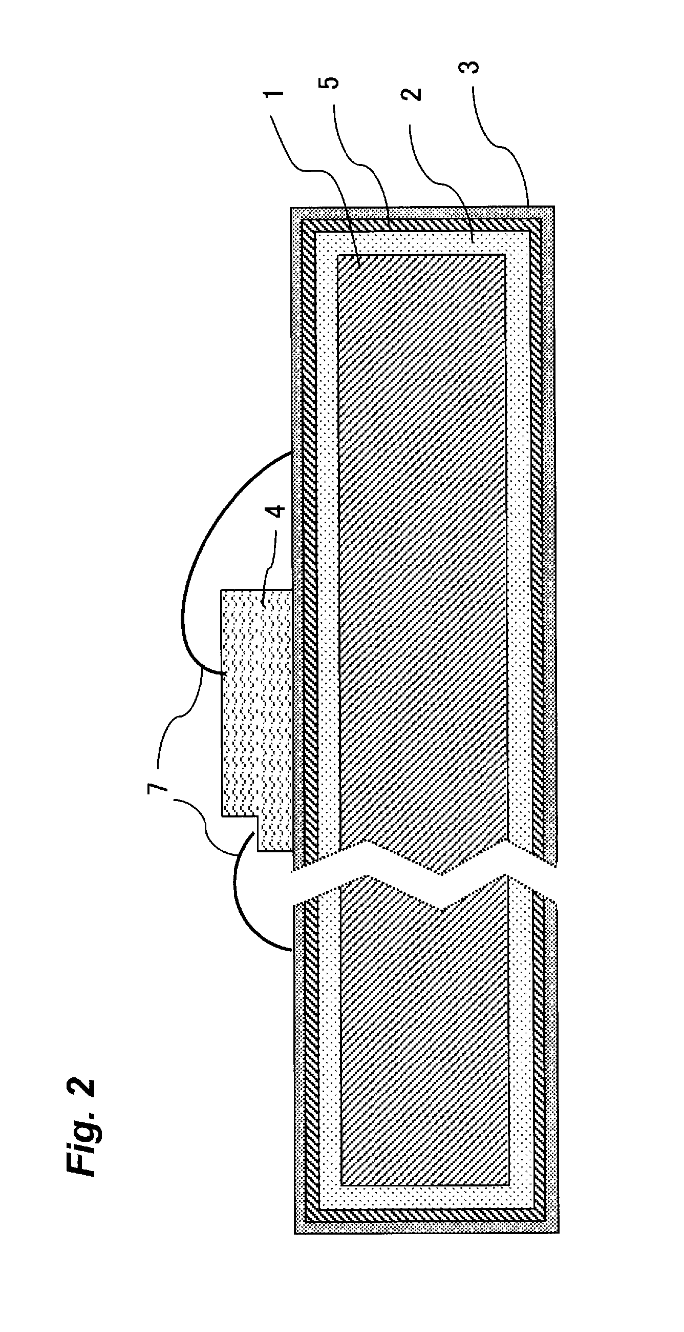
[0077]In Example No. 1, the respective electrically-conductive substrate, as shown in Tables 1-1 and 1-2, with thickness 0.2 mm and width 50 mm, was subjected to the following pretreatments, the following plating, and then the heat treatment under an atmospheric in the air at 100 to 200° C. for 1 to 48 hours, by using a thermostat (manufactured by ESPEC), thereby to obtain the lead frames of Examples 1 to 48 according to the present invention (Ex.), Conventional example 1 (Cony. ex.), and Comparative examples 1 to 10 (Comp. ex.), respectively, having the respective structure as shown in Tables 1-1 and 1-2. When the “reflow” treatment shown in the tables was performed, a silver layer and a layer of a metal other than silver (any one of In, Sn, and Sb) were formed, using the respective plating liquid in advance, followed by, before the heat treatment, subjecting the thus-formed layers to the reflow treatment, thereby to form a layer of a silver alloy (any one of Ag—In, Ag...


PUM

PropertyMeasurementUnit
Temperatureaaaaaaaaaa
Lengthaaaaaaaaaa
Fractionaaaaaaaaaa

Abstract

A lead frame for an optical semiconductor device, having: a layer 2 composed of silver or a silver alloy formed on an electrically-conductive substrate 1; a metal oxide layer 3 of a metal other than silver as an outer layer of the layer composed of silver or a silver alloy, wherein the metal oxide layer 3 is colorless and transparent or silver gray in color, and has a thickness thereof from 0.001 to 0.2 μm; a method of producing the same; and an optical semiconductor device utilizing the same.

Description

TECHNICAL FIELD[0001]The present invention relates to a lead frame for an optical semiconductor device, a method of producing the same, and an optical semiconductor device.BACKGROUND ART[0002]Lead frames for optical semiconductor devices have been widely used in constitution parts of light sources for various display and lighting, in which optical semiconductor elements (light-emitting elements), such as LEDs (light-emitting diodes), are utilized as the light sources. Such an optical semiconductor device is produced by, for example, arranging a lead frame as a substrate, mounting a light-emitting element on the lead frame, and sealing the light-emitting element and its surrounding with a resin, to prevent deterioration of the light-emitting element and its surrounded region by external factors, such as heat, humidity, and oxidization.[0003]When a LED element is used as a light source for lighting, there is a demand for reflective materials for lead frames to have a high reflectance ...

Claims


Application Information

Patent Timeline
IPC IPC(8): H01L33/62H05K5/02
CPCH01L33/60H01L33/62H01L2224/48091H01L2224/48227Y10T29/49121H01L2933/0066H01L2224/49107H01L2924/00014H01L23/495
Inventor KOBAYASHI, YOSHIAKIKOSEKI, KAZUHIROKIKUCHI, SHIN
Owner FURUKAWA ELECTRIC CO LTD
Why Eureka
Try Eureka