Junction field effect transistor structure with p-type silicon germanium or silicon germanium carbide gate(s) and method of forming the structure

a junction field effect transistor and gate structure technology, applied in the direction of transistors, electrical devices, semiconductor devices, etc., can solve the problems of high voff, difficult pinching off of the p-type top gate to the p-type bottom gate in the n-channel region without a high voltage, etc., and achieve the effect of reducing voff and fast pinching

Active Publication Date: 2012-07-05
GLOBALFOUNDRIES US INC
View PDF4 Cites 12 Cited by
  • Summary
  • Abstract
  • Description
  • Claims
  • Application Information

AI Technical Summary

Benefits of technology

[0005]In view of the foregoing, disclosed herein are embodiments of a junction field effect transistor (JFET) structure with one or more P-type silicon germanium (SiGe) or silicon germanium carbide (SiGeC) gates (i.e., a SiGe or SiGeC based heterojunction JFET). The P-type SiGe or SiGeC gate(s) allow for a lower pinch off voltage (i.e., lower Voff) without increasing the on resistance (Ron). Specifically, SiGe or SiGeC material in a P-type gate limits P-type dopant out diffusion and, thereby ensures that the P-type gate-to-N-type channel region junction is more clearly defined (i.e., abrupt as opposed to graded). By clearly defining this junction, the depletion layer in the N-type channel region is extended. Extending the depletion layer in turn allows for a faster pinch off (i.e., requires lower Voff). P-type SiGe or SiGeC gate(s) can be incorporated into conventional lateral JFET structures and / or vertical JFET structures. Also disclosed herein are embodiments of a method of forming such a JFET structure.

Problems solved by technology

Unfortunately, with current JFET structures there is a trade-off between Ron and Voff as a function of channel region doping and gate doping.
Specifically, doping to achieve low Ron typically results in a high Voff and vice versa.
On the one hand, the problem is accentuated in vertical JFET structures formed in deep sub-micro technologies and beyond, where a deep STI is deployed as a field for isolation.
Such a vertical JFETs exhibit high Voff because the P-type top gate is relatively shallow and the trench isolation structures that isolate the P-type top gate from the source / drain regions are relatively deep, thereby making pinch off of the P-type top gate to P-type bottom gate in the N-channel region difficult without a high voltage.

Method used


Image

  • Junction field effect transistor structure with p-type silicon germanium or silicon germanium carbide gate(s) and method of forming the structure
  • Junction field effect transistor structure with p-type silicon germanium or silicon germanium carbide gate(s) and method of forming the structure
  • Junction field effect transistor structure with p-type silicon germanium or silicon germanium carbide gate(s) and method of forming the structure

Examples


embodiment 200

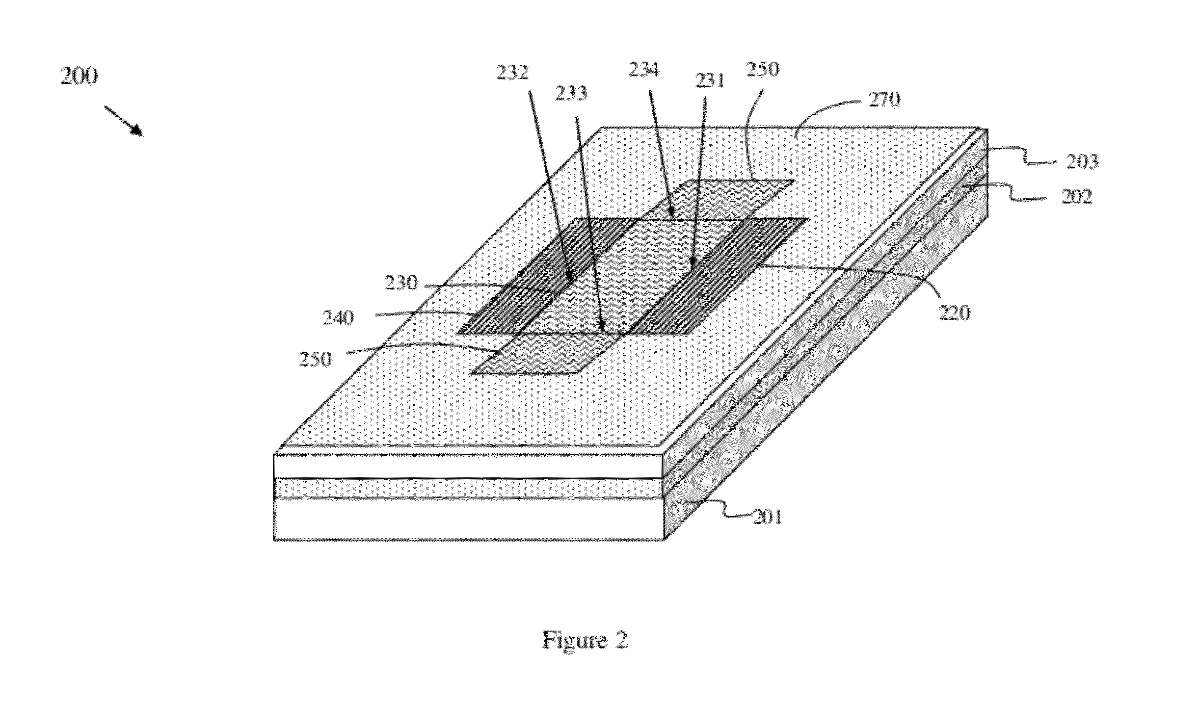
[0048]Referring to FIG. 2, one exemplary JFET embodiment 200 can comprise a semiconductor-on-insulator (SOI) lateral JFET structure. This lateral JFET structure 200 can comprise a semiconductor substrate 201 (e.g., a silicon substrate or other semiconductor substrate), an insulator layer 202 (e.g., a silicon oxide layer or other suitable insulator layer) on the substrate 201 and a semiconductor layer 203 (e.g., a single crystalline silicon layer or other suitable semiconductor layer) on the insulator layer 102. The semiconductor layer 203 can be N-type. That is, it can be doped with an N-type dopant.

[0049]In this embodiment, the N-type source / drain regions 250 can comprise N-type implant regions in the semiconductor layer 203 and the N-type channel region 230 can comprise a portion of the semiconductor layer 203 separating the N-type implant regions. Thus, the N-type source / drain regions 250 are positioned adjacent to opposing ends (i.e., first end 233 and second end 234) of the N-t...

embodiment 300

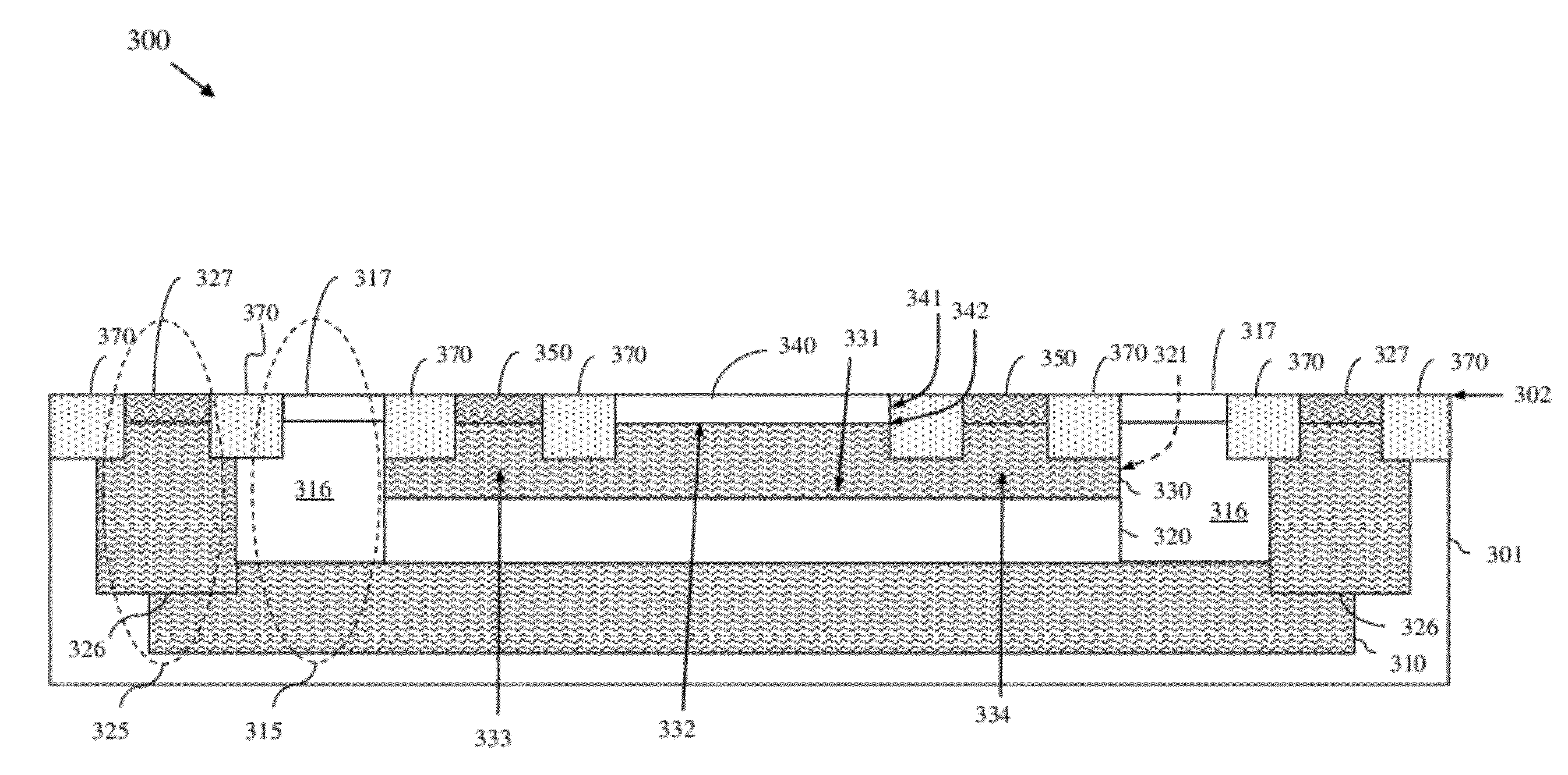
[0052]Referring to FIG. 3, another exemplary JFET embodiment 300 can comprise a vertical JFET. Specifically, this vertical JFET 300 can comprise a silicon substrate 300 (e.g., a P-type silicon substrate, such as a P- substrate) with a first N-well 310 buried therein.

[0053]The first P-type gate 320 can comprise a P-well in the substrate 301 above and abutting (i.e., in physical contact with) the first N-well 310. The N-type channel region 330 can comprise a second N-well in the substrate 301 above and abutting the P-well 320. The second P-type gate 340 can comprise a P-type silicon germanium layer or a P-type silicon germanium carbide layer filling a trench 341 that extends vertically from the top surface 302 of the substrate 301 into the second N-well 330 such that the bottom surface 342 of the trench 341 abuts the N-type channel region 330 and is above and physically separated from the first P-type gate 320. Additionally, the N-type source / drain regions 350 can comprise N-type impl...


PUM

PropertyMeasurementUnit
Ronaaaaaaaaaa
concentrationaaaaaaaaaa
ON resistanceaaaaaaaaaa

Abstract

Disclosed are embodiments of a junction field effect transistor (JFET) structure with one or more P-type silicon germanium (SiGe) or silicon germanium carbide (SiGeC) gates (i.e., a SiGe or SiGeC based heterojunction JFET). The P-type SiGe or SiGeC gate(s) allow for a lower pinch off voltage (i.e., lower Voff) without increasing the on resistance (Ron). Specifically, SiGe or SiGeC material in a P-type gate limits P-type dopant out diffusion and, thereby ensures that the P-type gate-to-N-type channel region junction is more clearly defined (i.e., abrupt as opposed to graded). By clearly defining this junction, the depletion layer in the N-type channel region is extended. Extending the depletion layer in turn allows for a faster pinch off (i.e., requires lower Voff). P-type SiGe or SiGeC gate(s) can be incorporated into conventional lateral JFET structures and/or vertical JFET structures. Also disclosed herein are embodiments of a method of forming such a JFET structure.

Description

BACKGROUND[0001]1. Field of the Invention[0002]The present invention relates to junction field effect transistors (JFETs), and more specifically, to a JFET structure with one or more P-type silicon germanium or silicon germanium carbide gates and a method of forming the structure.[0003]2. Description of the Related Art[0004]Junction field effect transistors (JFETs) are often incorporated into integrated circuits and, particularly, into high speed portable devices, as resistors for power switching regulation. Ideally, such a JFET will have a low ON resistance (i.e., low resistance in the ON state, low Ron) and will also only require a low pinch off voltage (i.e., a low voltage to achieve the OFF state, low Voff). Unfortunately, with current JFET structures there is a trade-off between Ron and Voff as a function of channel region doping and gate doping. Specifically, doping to achieve low Ron typically results in a high Voff and vice versa. On the one hand, the problem is accentuated ...

Claims


Application Information

Patent Timeline
Patent Type & Authority Applications(United States)
IPC IPC(8): H01L29/80H01L21/335
CPCH01L29/42316H01L29/808H01L29/66916H01L29/8086H01L29/66462H01L27/14679H01L29/16H01L29/0649
Inventor LIU, XUEFENGPHELPS, RICHARD A.RASSEL, ROBERT M.TIAN, XIAOWEI
Owner GLOBALFOUNDRIES US INC
Why Eureka
Try Eureka