Method for making epitaxial structure
a technology of epitaxial structure and method, which is applied in the direction of crystal growth process, polycrystalline material growth, transportation and packaging, etc., can solve the problems of difficult fabrication of devices with small feature sizes, difficult to use sapphire substrates, and complex process of lithography and etching
- Summary
- Abstract
- Description
- Claims
- Application Information
AI Technical Summary
Problems solved by technology
Method used
Image

Examples
example 1
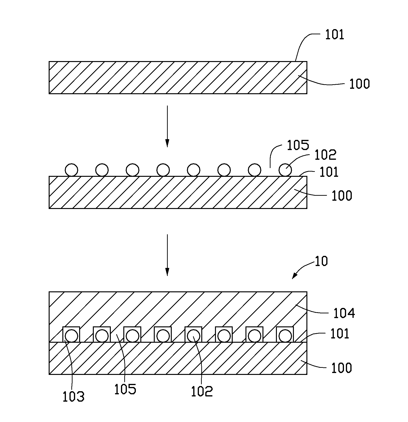
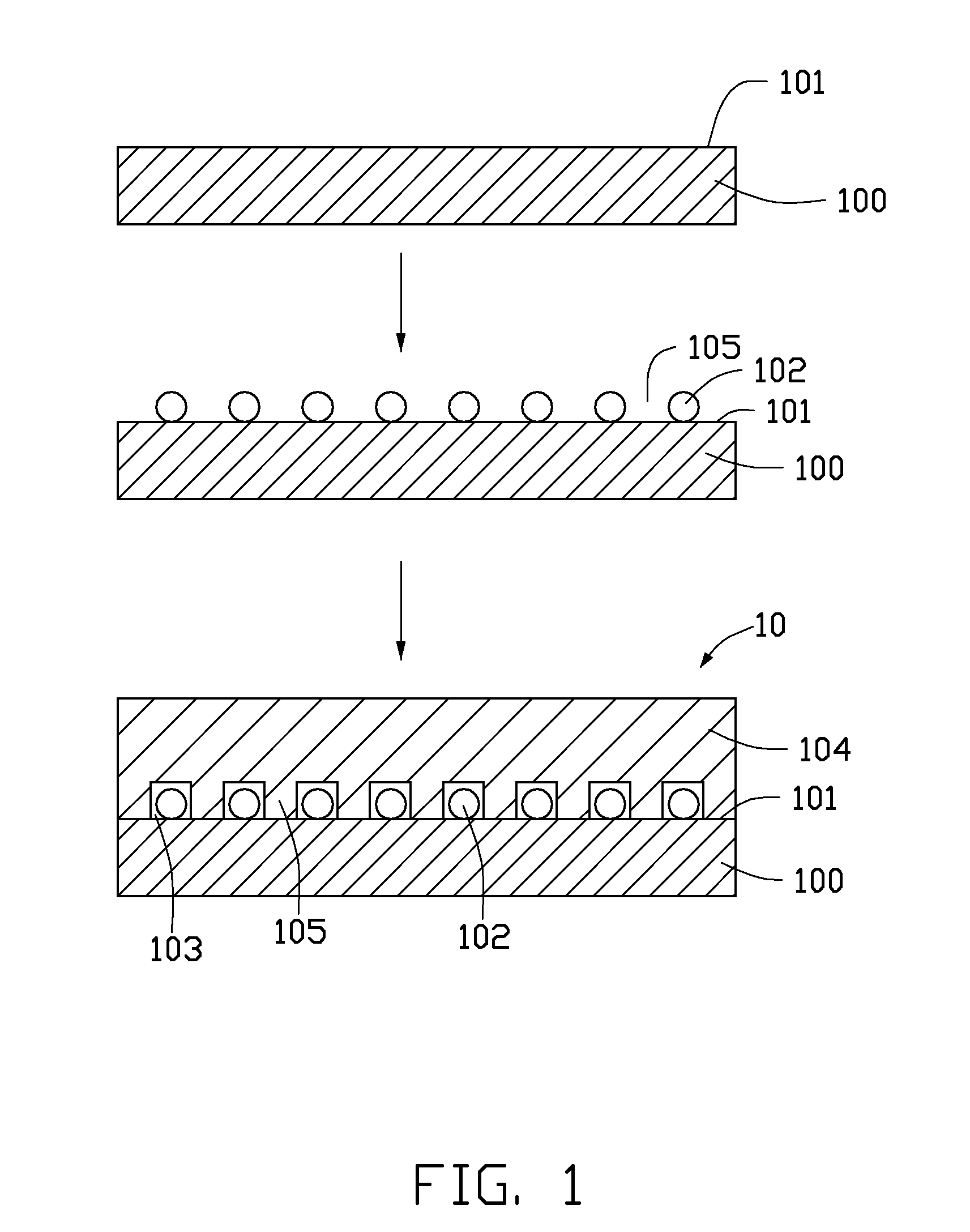
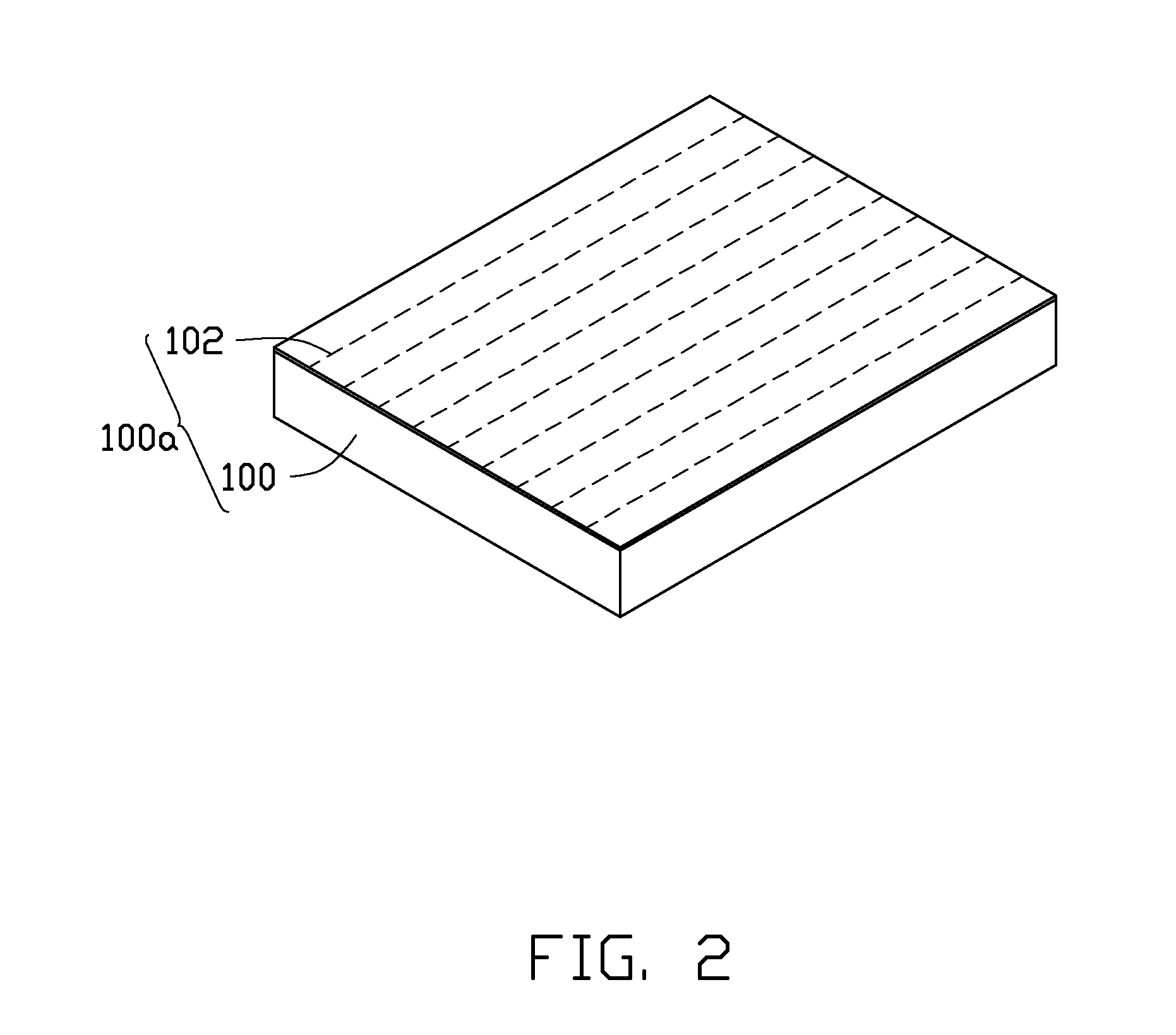
[0218]In example 1, the substrate is a SOI, the epitaxial layer is a GaN layer and grown on the SOI substrate by a MOCVD method. The nitrogen source gas is high-purity ammonia (NH3), the Ga source gas is trimethyl gallium (TMGa) or triethyl gallium (TEGa), and the carrier gas is hydrogen (H2). A single drawn carbon nanotube film is placed on an epitaxial growth surface of the SOI substrate. The growth of the epitaxial layer includes the following steps:
[0219]step (a), putting the SOI substrate with the drawn carbon nanotube film thereon into a vacuum reaction chamber and heating the reaction chamber to a temperature of about 1070° C.;
[0220]step (b), introducing the nitrogen source gas and the Ga source gas into the vacuum reaction chamber with the carrier gas;
[0221]step (c), vertical epitaxially growing a plurality of GaN epitaxial grains for about 450 seconds at about 1070° C.;
[0222]step (d), heating the reaction chamber to about 1110° C., reducing the flow of the Ga source gas, ke...
example 2
[0225]In example 2, the substrate is sapphire, the epitaxial layer is grown on the sapphire substrate by MOCVD method. The nitrogen source gas is high-purity ammonia (NH3), the Ga source gas is trimethyl gallium (TMGa) or triethyl gallium (TEGa), and the carrier gas is hydrogen (H2). A single drawn carbon nanotube film is placed on an epitaxial growth surface of the sapphire substrate. The growth of the epitaxial layer includes the following steps:
[0226]step (a), locating the sapphire substrate with the single drawn carbon nanotube film thereon into a reaction chamber, heating the sapphire substrate to about 1100° C. to about 1200° C., introducing the carrier gas, and baking the sapphire substrate for about 200 seconds to about 1000 seconds;
[0227]step (b), growing a low-temperature GaN buffer layer with a thickness of about 10 nanometers to about 50 nanometers by cooling down the temperature of the reaction chamber to a range from about 500° C. to 650° C. in the carrier gas atmosphe...
example 3
[0231]Example 3 is similar to example 2 described above except that a step (e) of irradiating the epitaxial structure with a laser beam in air is performed after step (d). In step (e), the drawn carbon nanotube film is removed by oxidation. The laser beam is provided by a carbon dioxide laser device. The power of the laser device is about 30 watts. The wavelength of the laser is about 10.6 micrometers. The diameter of the laser spot is about 3 millimeters. The power density of the laser is about 0.053×10¹² watts per square meter. The irradiating time is less than 1.8 seconds.
PUM
 Abstract
Description
Claims
Application Information
 - R&D
- Intellectual Property
- Life Sciences
- Materials
- Tech Scout
- Unparalleled Data Quality
- Higher Quality Content
- 60% Fewer Hallucinations
Browse by: Latest US Patents, China's latest patents, Technical Efficacy Thesaurus, Application Domain, Technology Topic, Popular Technical Reports.
© 2025 PatSnap. All rights reserved.Legal|Privacy policy|Modern Slavery Act Transparency Statement|Sitemap|About US| Contact US: help@patsnap.com