Vertical parasitic pnp device in a silicon-germanium hbt process and manufacturing method of the same

a technology of silicon-germanium hbt and pnp device, which is applied in the direction of semiconductor devices, basic electric elements, electrical equipment, etc., can solve the problems of large connection resistance of collector electrodes, large device area, and greatly limited further reduction of device size, so as to achieve effective reduction of collector resistance of devices, good frequency characteristics, and large current amplification factor

Inactive Publication Date: 2012-07-19
SHANGHAI HUAHONG GRACE SEMICON MFG CORP
View PDF4 Cites 7 Cited by
  • Summary
  • Abstract
  • Description
  • Claims
  • Application Information

AI Technical Summary

Benefits of technology

[0005]An objective of the present invention is to provide a vertical parasitic PNP device in a SiGe HBT process, which can be used as an output device in a high-speed and high-gain HBT circuit, thus providing an alternative choice for the circuit. The vertical parasitic PNP device in a SiGe HBT process can effectively reduce the device area and the collector resistance of the PNP device, and improve the device performance. The present invention also provides a manufacturing method of vertical parasitic PNP device in a SiGe HBT process, which does not need additional process conditions and therefore can reduce manufacturing costs.
[0025]The vertical parasitic PNP device in a SiGe HBT process of the present invention has a relatively large current amplification factor and relatively good frequency characteristics, and therefore can be used as an output device in a high-speed and high-gain HBT circuit, providing an alternative choice for the circuit. The device of the present invention adopts an advanced deep hole contact process to form deep hole contacts directly contacting with the P-type pseudo buried layers to pick up the collector electrodes of the device, which can effectively reduce the device area. Due to the reduction of distances between the pick-up positions and the collector region, and also due to the heavily doped P-type pseudo buried layers, the collector resistance of the device is effectively reduced, and thus frequency characteristics of the PNP device are improved. By using a polysilicon emitter electrode, the base current of the device can be reduced while maintaining the collector current unchanged, so that the current gain of the PNP device is improve. The manufacturing method of the present invention uses process conditions of an existing SiGe HBT process, and thus can reduce manufacturing costs.

Problems solved by technology

The device has disadvantages such as a large device area and a large connection resistance of the collector electrode.
As in prior arts the collector electrode needs to be picked up through another active area adjacent to the collector region, and STI or other field oxide regions are needed to separate the another active area from the collector region, further reduction of the device size is greatly limited.

Method used


Image

  • Vertical parasitic pnp device in a silicon-germanium hbt process and manufacturing method of the same
  • Vertical parasitic pnp device in a silicon-germanium hbt process and manufacturing method of the same
  • Vertical parasitic pnp device in a silicon-germanium hbt process and manufacturing method of the same

Examples


Embodiment Construction

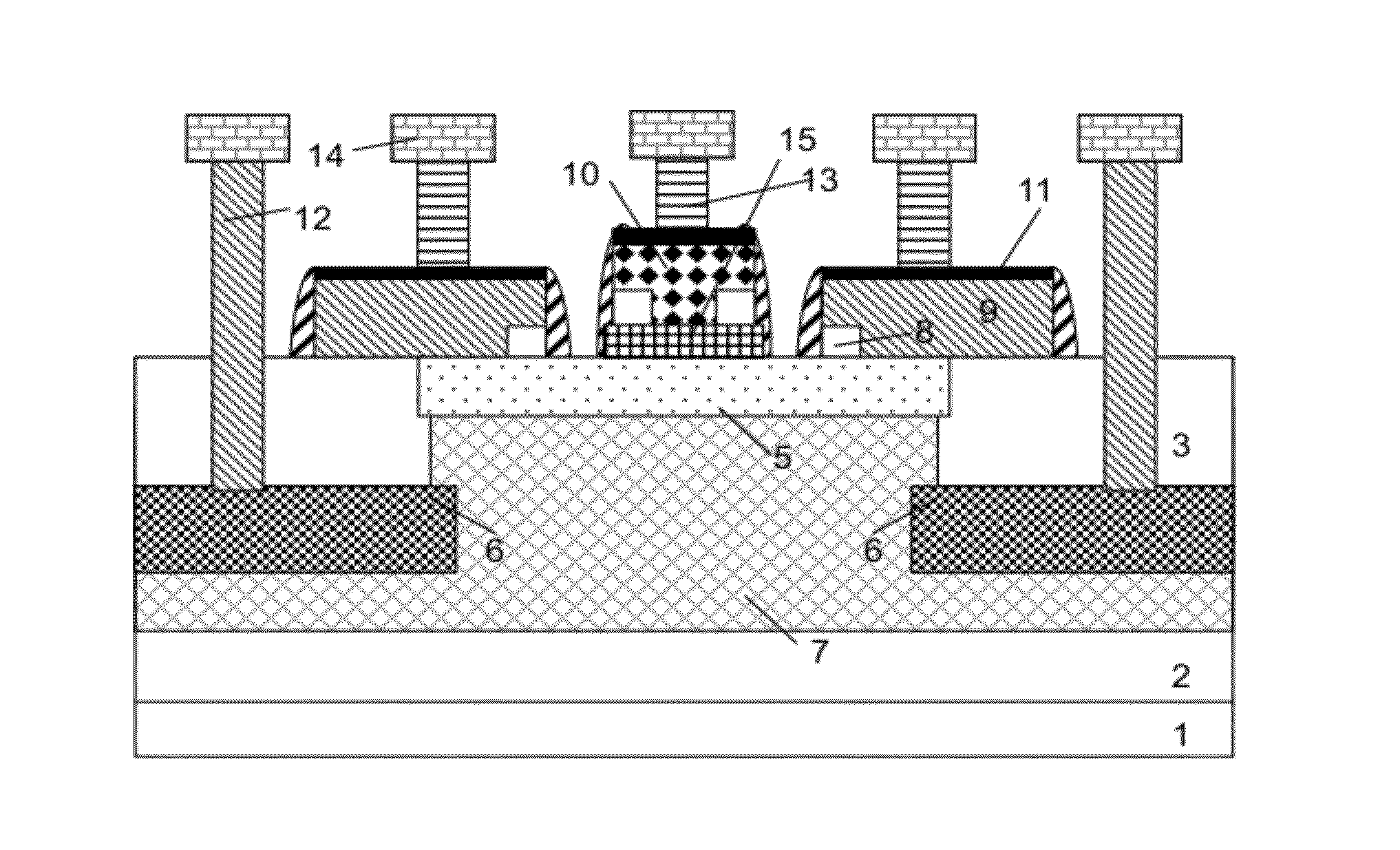
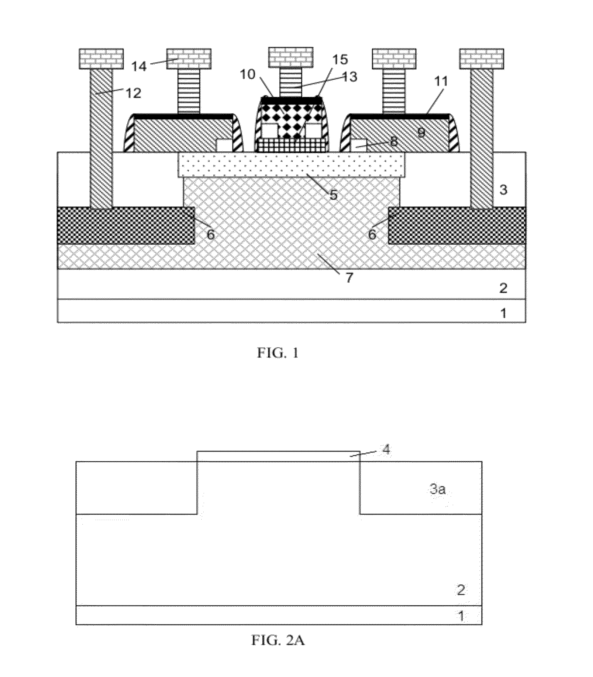
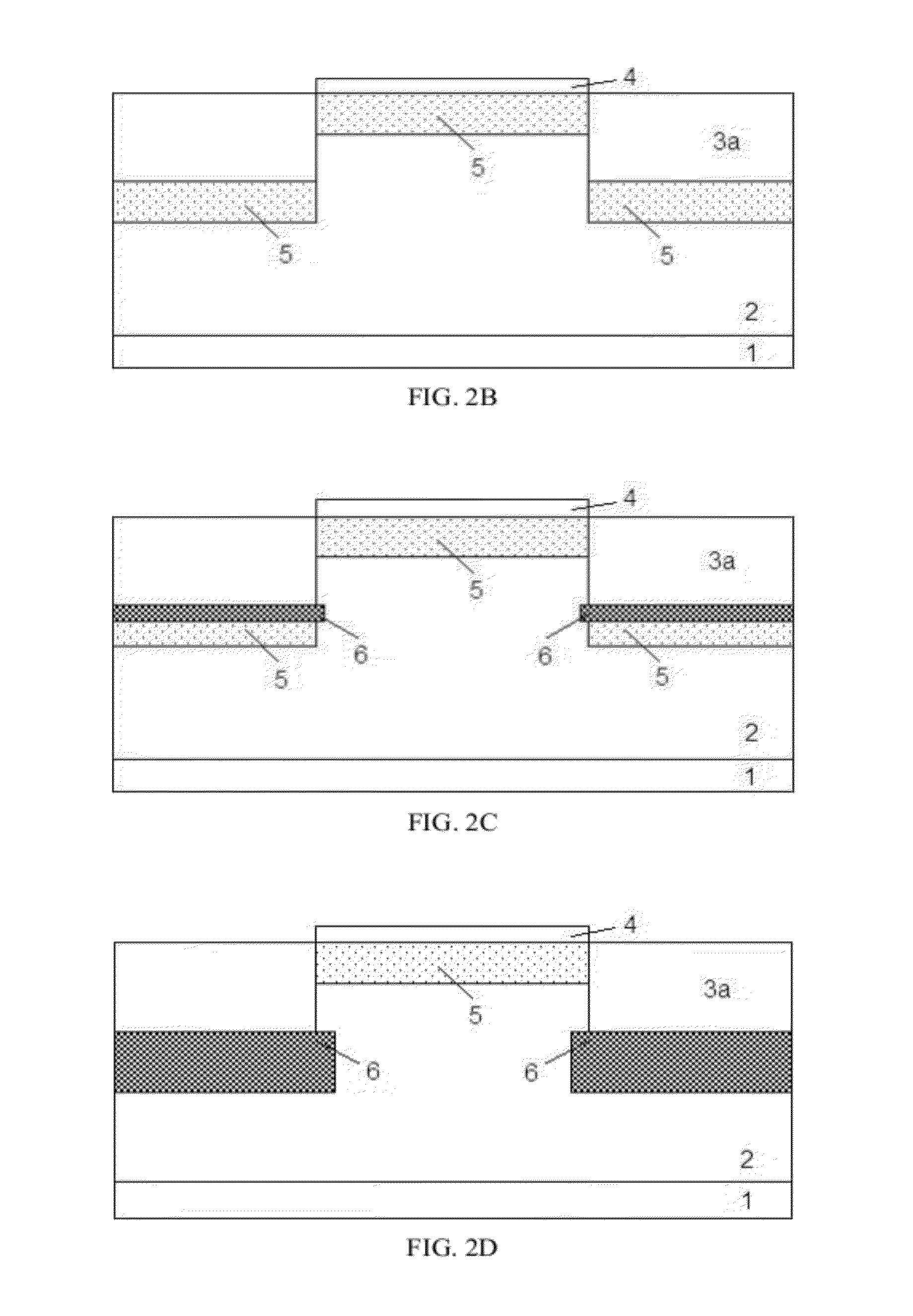
[0031]FIG. 1 shows the structure of a vertical parasitic PNP device in a BiCMOS process according to an embodiment of the present invention. The vertical parasitic PNP device is formed on a P-type silicon substrate 1, wherein, an N-type deep well 2 is formed on the P-type silicon substrate 1, and an active area is isolated by shallow trench field oxide fields 3, i.e. shallow trench isolations (STI). The vertical parasitic PNP device comprises:

[0032]A collector region 7, comprising a P-type ion implantation region formed in the active area; the collector region 7 has a depth larger than or equal to those of bottoms of the shallow trench field oxide regions 3. The P-type ion implantation region of the collector region 7 is implanted by using boron impurities with two implantation steps: in the first step, implantation dose is 1e11 cm−2˜5e13 cm−2 and implantation energy is 100 KeV˜300 KeV; in the second step, implantation dose is Sell cm−2˜1e13 cm−2 and implantation energy is 30 KeV˜10...


PUM


Abstract

A vertical parasitic PNP device in a SiGe HBT process is disclosed which comprises a collector region, a base region, an emitter region, P-type pseudo buried layers and N-type polysilicons. The pseudo buried layers are formed at bottom of shallow trench field oxide regions around the collector region and contact with the collector region; deep hole contacts are formed on top of the pseudo buried layers to pick up collector electrodes. The N-type polysilicons are formed on top of the base region and are used to pick up base electrodes. The emitter region comprises a P-type SiGe epitaxial layer and a P-type polysilicon both of which are formed on top of the base region. A manufacturing method of a vertical parasitic PNP device in a SiGe HBT process is also disclosed.

Description

CROSS-REFERENCES TO RELATED APPLICATIONS[0001]This application claims the priority of Chinese patent application number 201110006703.1, filed on Jan. 13, 2011, the entire contents of which are incorporated herein by reference.TECHNICAL FIELD[0002]The present invention relates to the field of semiconductor integrated circuit manufacturing, and in particular, relates to a vertical parasitic PNP device in a silicon-germanium heterojunction bipolar transistor (SiGe HBT) process. The present invention also relates to a manufacturing method of vertical parasitic PNP device in a SiGe HBT process.BACKGROUND OF THE INVENTION[0003]Higher and higher cut-off frequency of the device is demanded in the application of radio-frequency (RF). In BiCMOS process technology, NPN transistors, especially silicon-germanium heterojunction bipolar transistors (SiGe HBTs) or silicon-germanium-carbon heterojunction bipolar transistors (SiGeC HBTs), have become good choices for ultra high frequency devices. Mor...

Claims


Application Information

Patent Timeline
Patent Type & Authority Applications(United States)
IPC IPC(8): H01L29/737H01L21/331
CPCH01L29/0821H01L29/16H01L21/76237H01L29/7371H01L29/66242
Inventor CHEN, FANCHEN, XIONGBIN
Owner SHANGHAI HUAHONG GRACE SEMICON MFG CORP
Why Eureka
Try Eureka