Semiconductor memory device

a semiconductor and memory device technology, applied in semiconductor devices, instruments, electrical devices, etc., can solve the problems of matrix driving difficulty, insufficient on/off ratio of transistors, and difficulty in setting channel lengths less than or equal to 20 nm, so as to achieve the effect of small channel length

Active Publication Date: 2012-07-19
SEMICON ENERGY LAB CO LTD
View PDF15 Cites 5 Cited by
  • Summary
  • Abstract
  • Description
  • Claims
  • Application Information

AI Technical Summary

Benefits of technology

[0027]Accordingly, even if the thickness of the floating gate insulating film is made thinner than ever, leakage of electric charge from the floating gate due to a tunnel effect can be prevented. By making the thickness of the floating gate insulating film smaller, the channel length can be made small. For example, when the thickness of the floating gate insulating film is 2 nm, an FG memory device having a channel length of 7 nm can be manufactured.

Problems solved by technology

On the other hand, when the thickness of the floating gate insulating film is greater than 6 nm, it is difficult to set the channel length to less than or equal to 20 nm.
Even if the channel length is set to less than or equal to 20 nm, due to a short channel effect, the on / off ratio of a transistor cannot be sufficiently high, which leads to difficulty in matrix driving.

Method used


Image

  • Semiconductor memory device
  • Semiconductor memory device
  • Semiconductor memory device

Examples


embodiment 1

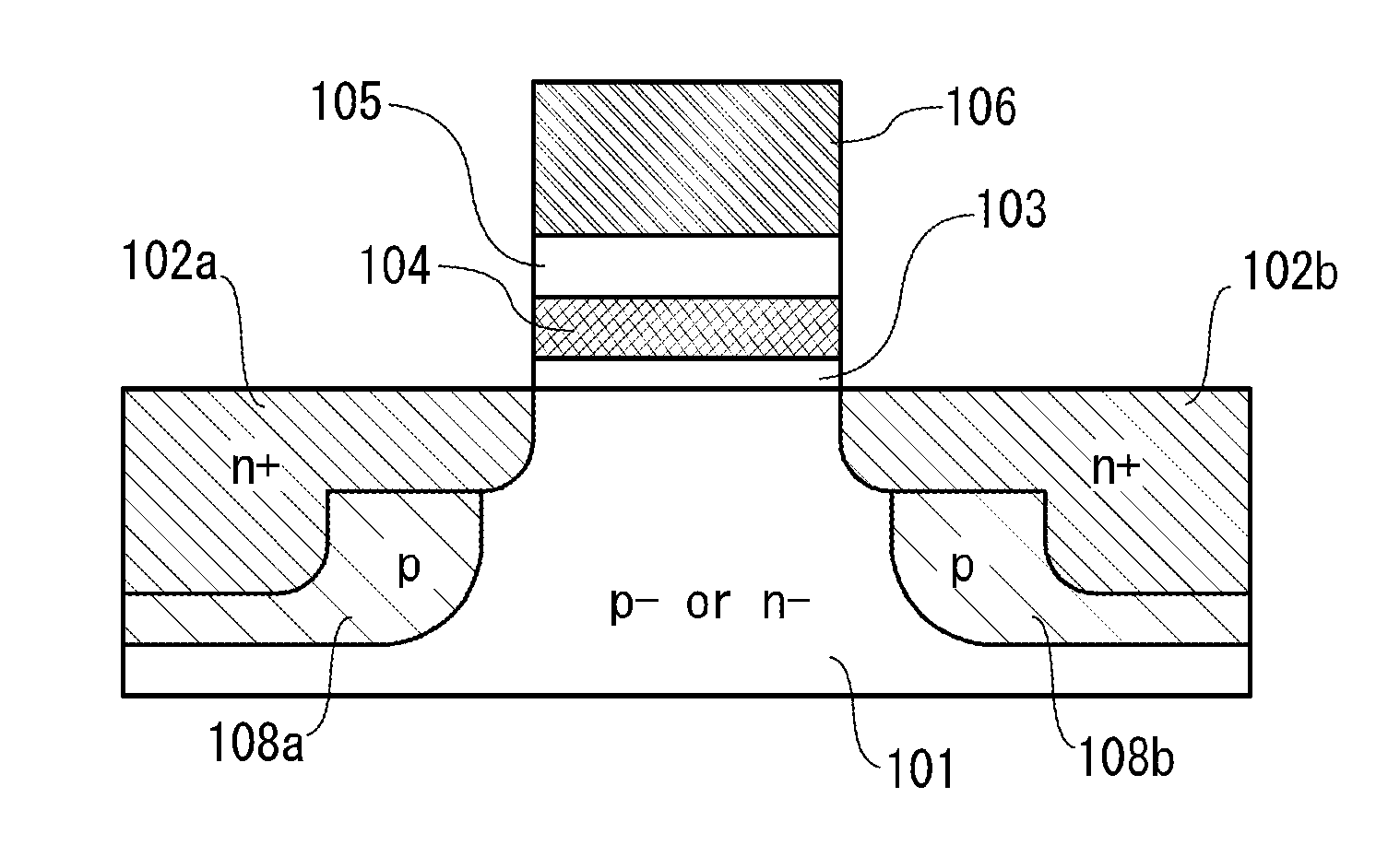
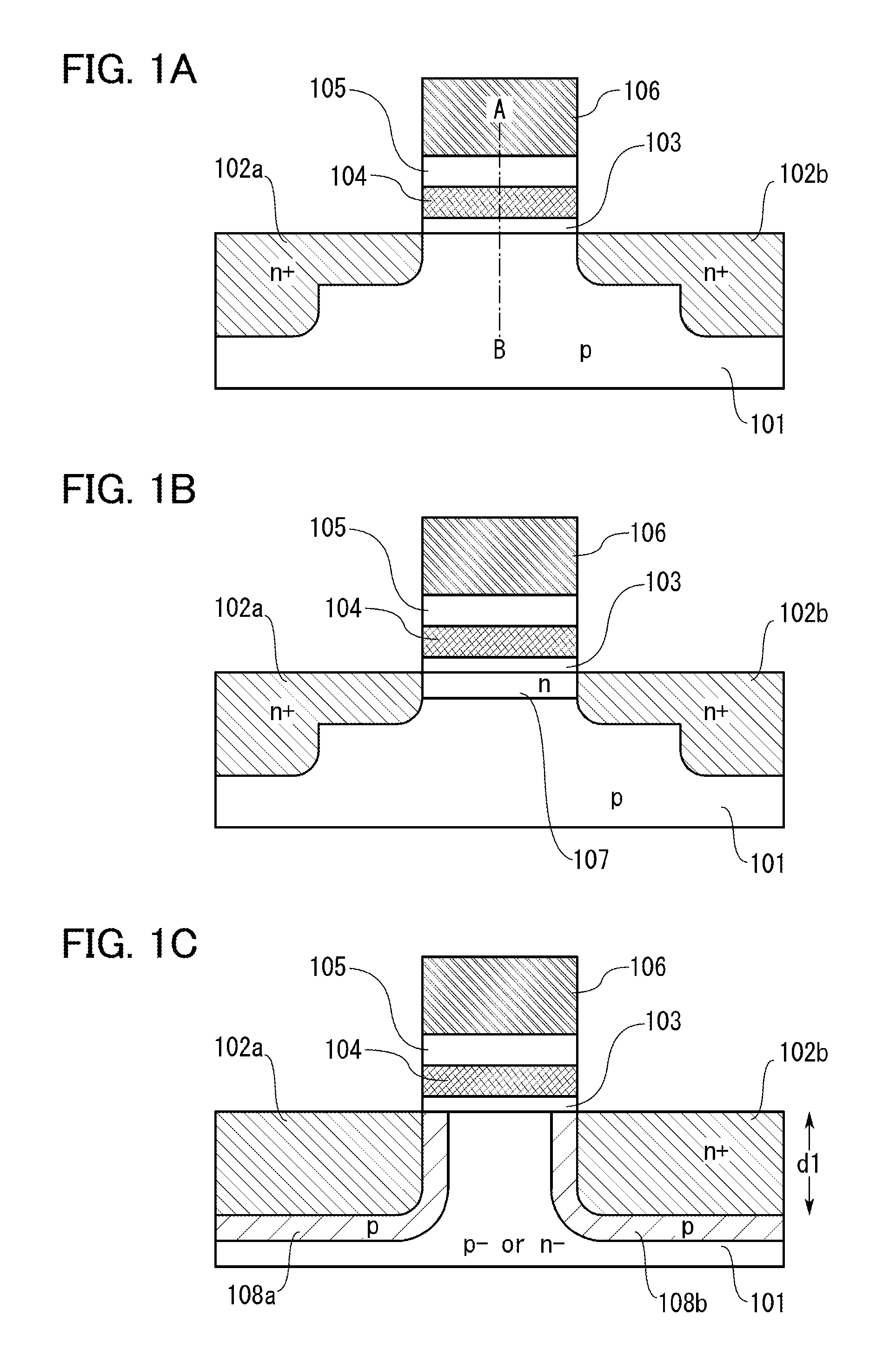
[0036]FIG. 1A illustrates an example of an FG memory device in this embodiment. Here, a schematic cross-sectional view of a transistor in a channel direction is illustrated. The transistor includes a floating gate 104 including a high-work-function compound semiconductor having a thickness of greater than or equal to 5 nm and less than or equal to 100 nm over a substrate 101 of p-type single crystal silicon, and includes a floating gate insulating film 103 with an appropriate thickness between the floating gate 104 and the substrate 101.

[0037]Note that for the substrate 101, a semiconductor material such as germanium, gallium arsenide, or gallium antimonide which has an electron affinity of 3.5 eV to 4.5 eV and a band gap of less than or equal to 1.5 eV can be used other than silicon.

[0038]The width of the floating gate 104, which is important in determining the channel length of the transistor, is set to less than or equal to 50 nm, preferably less than or equal to 20 nm. Further, ...

embodiment 2

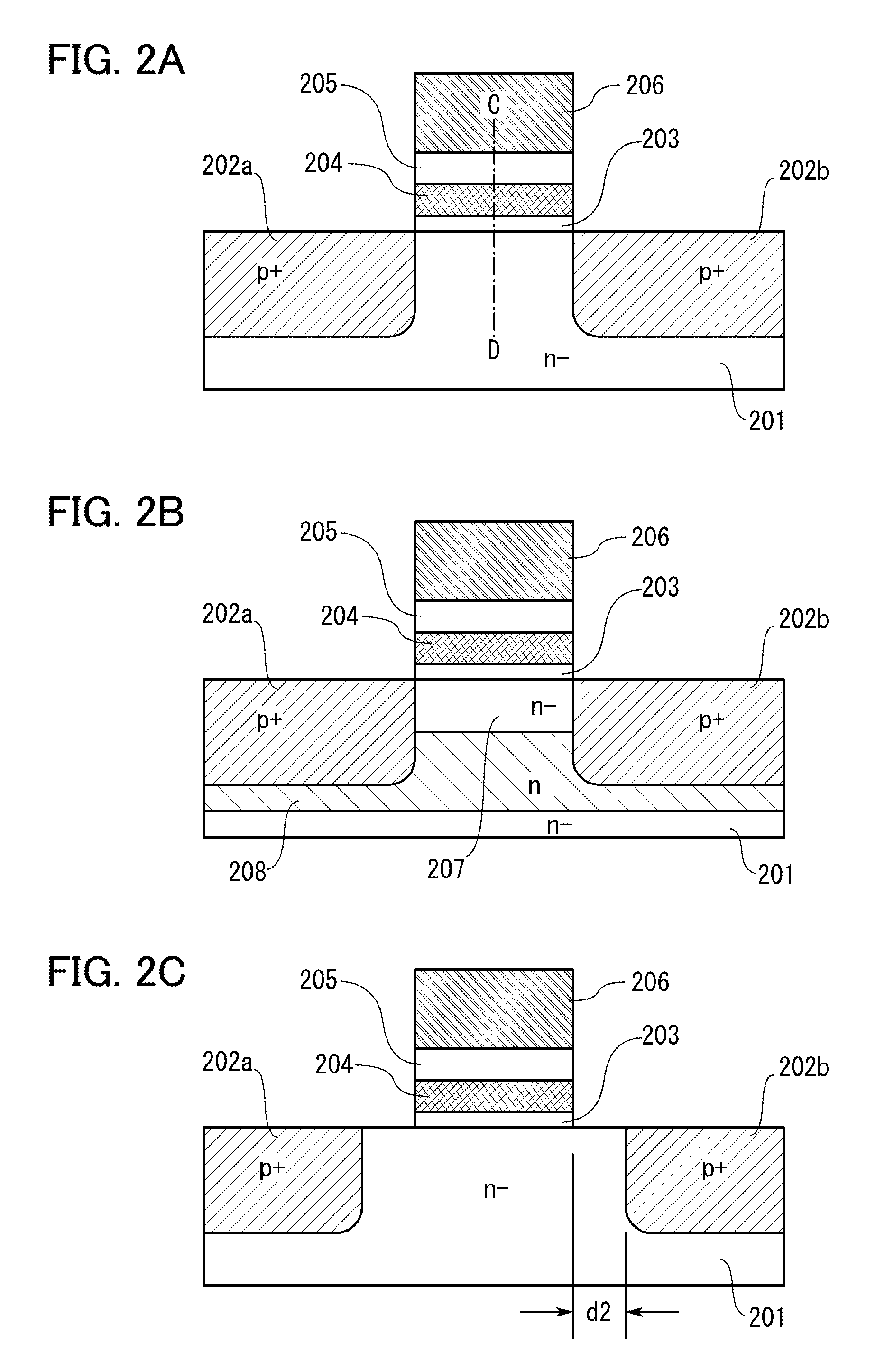
[0059]FIG. 2A illustrates an example of an FG memory device of this embodiment. Note that Embodiment 1 can be referred to for part of descriptions. Here, a schematic cross-sectional view of a transistor in a channel direction is illustrated. The transistor includes a floating gate 204 formed using a high-work-function compound semiconductor having a thickness of greater than or equal to 5 nm and less than or equal to 100 nm over an n-type single crystal silicon substrate 201, and includes a floating gate insulating film 203 having an appropriate thickness between the floating gate 204 and the substrate 201.

[0060]The width of the floating gate 204 is less than or equal to 50 nm, preferably less than or equal to 20 nm, more preferably less than or equal to 10 nm. Further, the thickness of the floating gate insulating film 203 is preferably set to 2 nm to 4 nm.

[0061]The substrate 201 is doped with p-type impurities to form a source 202a and a drain 202b. A control gate 206 is provided ...

embodiment 3

[0065]An example of a method for manufacturing an FG memory device having both characteristics of the FG memory devices illustrated in FIGS. 2B and 2C will be described with reference to FIGS. 3A to 3C. Many steps can be performed in accordance with known semiconductor techniques; therefore, as for the details, the known techniques can be used as a reference.

[0066]First, a portion of the n-type high-resistance single crystal silicon substrate 201 (the impurity concentration is 1×1013 cm−3 to 1×1017 cm−3) to the depth of 10 nm to 200 nm is doped with n-type impurities to form the n-type region 208. As an n-type impurity element, an element which can control the depth precisely, such as arsenic, is used, and the impurity concentration may be 1×1018 cm−3 to 1×1020 cm−3. As a result, the weak n-type region 207 (having the same impurity concentration as the substrate 201) is formed in a shallow portion in the vicinity of the surface of the substrate.

[0067]Alternatively, the weak n-type r...


PUM


Abstract

To provide a semiconductor memory device having a floating gate which operates with a short channel. A high-work-function compound semiconductor having a work function of greater than or equal to 5.5 eV, such as indium nitride or zinc nitride, is used for the floating gate. Accordingly, the potential barrier of the floating gate insulating film between the substrate and the floating gate is higher than that of a conventional one, so that leakage of electric charge due to a tunnel effect can be reduced even if the thickness of the floating gate insulating film is made small. Since the thickness of the floating gate insulating film can be made small, the channel can be further shortened.

Description

BACKGROUND OF THE INVENTION[0001]1. Field of the Invention[0002]The present invention relates to a floating-gate semiconductor memory device.[0003]2. Description of the Related Art[0004]In recent years, semiconductor memory devices such as flash memories which store data by accumulation of electric charge in floating gates (hereinafter, referred to as FG memory devices) have been used for many electronic devices, home appliances, and the like. FG memory devices are highly integrated, and in accordance with that, cost per bit is reduced.[0005]Although silicon has been often used for floating gates conventionally (for example, see Patent Document 1), in recent years, attempts to use materials other than silicon have been reported (for example, see Non-Patent Document 1). In addition, use of semiconductor particles instead of floating gates has been proposed (for example, see Patent Documents 2 and 3).REFERENCEPatent Document[0006][Patent Document 1] U.S. Pat. No. 6,815,755[0007][Paten...

Claims


Application Information

Patent Timeline
Patent Type & Authority Applications(United States)
IPC IPC(8): H01L29/788
CPCG11C16/04H01L29/7881H01L21/28273H01L29/40114H01L29/513H01L29/517
Inventor TAKEMURA, YASUHIKO
Owner SEMICON ENERGY LAB CO LTD
Why Eureka
Try Eureka