Method for manufacturing semiconductor device

a semiconductor and manufacturing technology, applied in the direction of semiconductor devices, electrical equipment, transistors, etc., can solve the problems of small power consumption of the display device in which a transistor including an oxide semiconductor is used, and achieve the effects of low leakage current, excellent electrical characteristics, and small channel length

Active Publication Date: 2017-12-26
SEMICON ENERGY LAB CO LTD
View PDF191 Cites 0 Cited by
  • Summary
  • Abstract
  • Description
  • Claims
  • Application Information

AI Technical Summary

Benefits of technology

[0009]An object is to provide a minute shape. Another object is to provide a transistor with a small channel length. Another object is to provide a transistor with a small subthreshold swing value. Another object is to provide a transistor having a small short-channel effect. Another object is to provide a transistor with normally-off electrical characteristics. Another object is to provide a transistor having a low leakage current in an off state. Another object is to provide a transistor with excellent electrical characteristics. Another object is to provide a highly reliable transistor. Another object is to provide a transistor with high frequency characteristics.
[0014]A minute shape can be provided. A transistor with a small channel length can be provided. A transistor with a small subthreshold swing value can be provided. A transistor having a small short-channel effect can be provided. A transistor with normally-off electrical characteristics can be provided. A transistor having a low leakage current in an off state can be provided. A transistor with excellent electrical characteristics can be provided. A highly reliable transistor can be provided. A transistor with high frequency characteristics can be provided.

Problems solved by technology

For example, a display device in which a transistor including an oxide semiconductor is used is known to have small power consumption.

Method used


Image

  • Method for manufacturing semiconductor device
  • Method for manufacturing semiconductor device
  • Method for manufacturing semiconductor device

Examples


example 1

[0486]In this example, an example in which the processing method of one embodiment of the present invention is used is described.

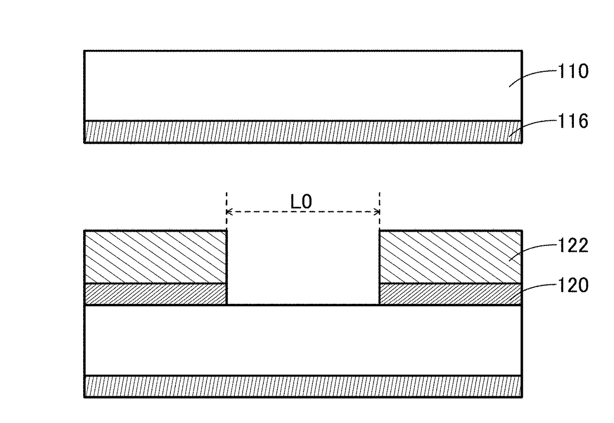
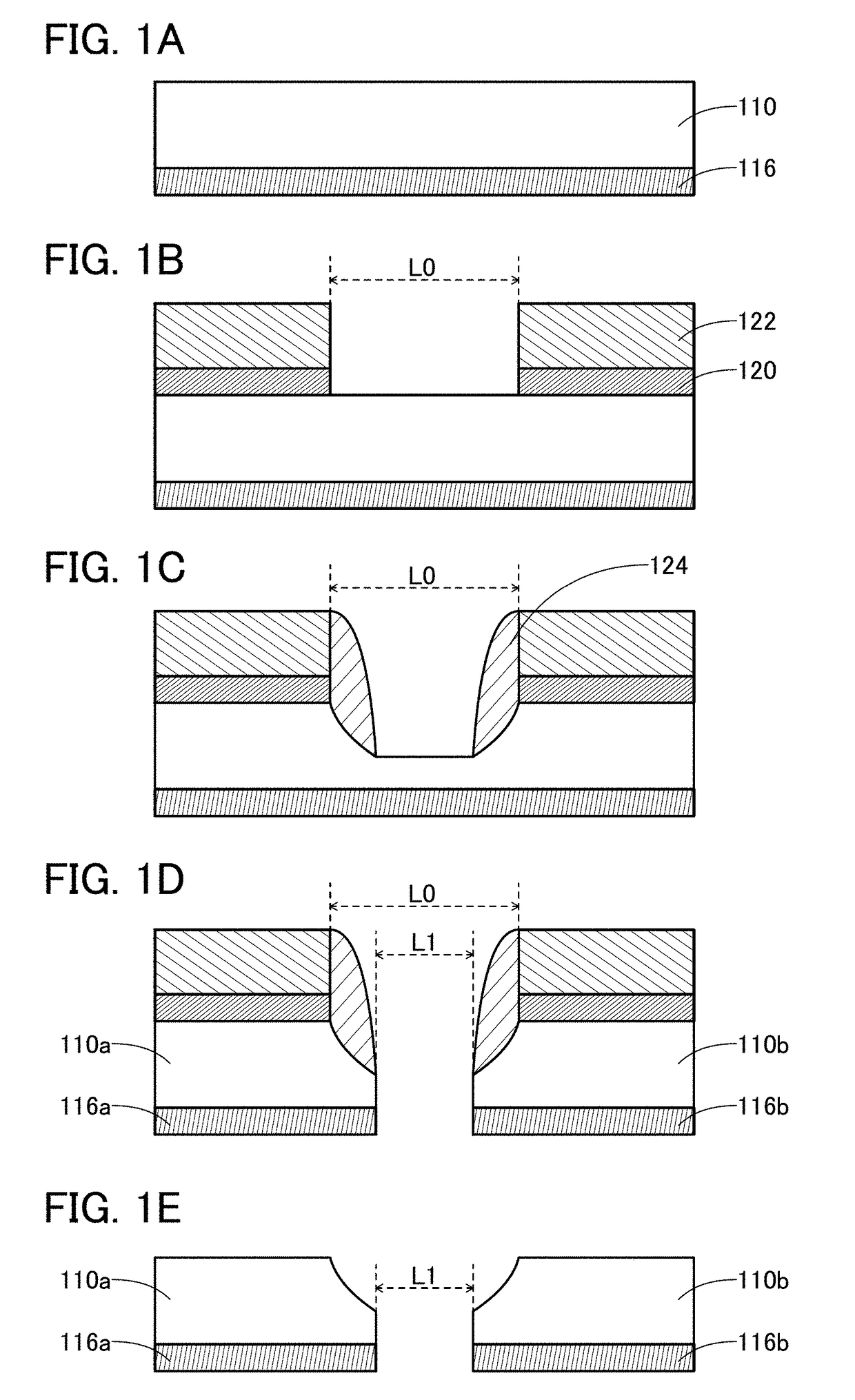
[0487]First, a 126.6-mm-square silicon substrate was prepared. Next, a 400-nm-thick silicon oxide was formed by a thermal oxidation method. Then, a 40-nm-thick In—Ga—Zn oxide was formed by a sputtering method. After that, a 50-nm-thick tungsten film was formed by a sputtering method.

[0488]Subsequently, a 170-nm-thick BARC was formed. Next, a resist was formed. Then, a resist was exposed to light using a photomask. After that, the resist was developed to form a groove with a size of 300 nm.

[0489]Subsequently, plasma was generated using a trifluoromethane gas at a flow rate of 50 sccm and a helium gas at a flow rate of 100 sccm, and plasma treatment was performed. Note that the pressure was 5.5 Pa, the substrate temperature was 70° C., the ICP power was 475 W, the bias power was 300 W, and the process time was 80 seconds. At that time, an organic substance w...

example 2

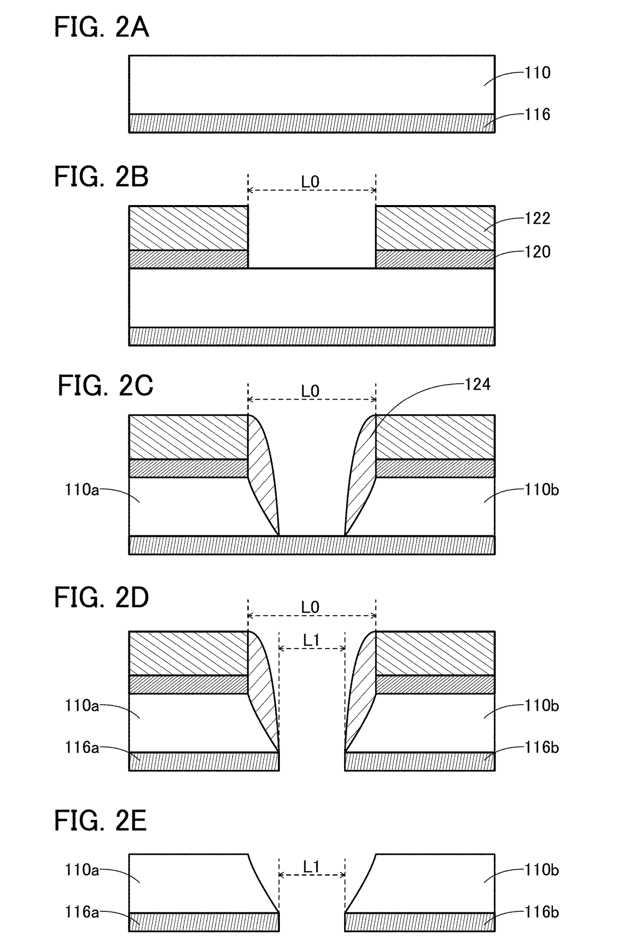
[0496]In this example, a transistor with a reduced channel length was fabricated with the use of the tungsten films described in Example 1 as the source and drain electrodes of the transistor.

[0497]FIGS. 48A and 48B illustrate the structure of the fabricated transistor. FIG. 48A is a top view of the transistor, and FIG. 48B is a cross-sectional view thereof taken along dashed dotted lines G1-G2 and G3-G4 in FIG. 48A. Since the structure of the transistor in FIGS. 48A and 48B is similar to that of the transistor illustrated in FIG. 12A, the same reference numerals are used. Furthermore, in a manner similar to that illustrated in FIGS. 13C and 13D, the semiconductors 406a and 406c were provided above and below the semiconductor 406.

[0498]A 126.6-mm-square silicon substrate was used as the substrate 400. As the insulator 402, a stack of a 100-nm-thick silicon oxide and a 300-nm-thick silicon oxynitride was used. As the semiconductor 406a, a 20-nm-thick In—Ga—Zn oxide formed using an In...


PUM


Abstract

A method for manufacturing a semiconductor device, including the steps of forming a semiconductor over a substrate; forming a first conductor over the semiconductor; forming a first insulator over the first conductor; forming a resist over the first insulator; performing light exposure and development on the resist to make a second region and a third region remain and expose part of the first insulator; applying a bias in a direction perpendicular to a top surface of the substrate and generating plasma using a gas containing carbon and halogen; and depositing and etching an organic substance with the plasma. The etching rate of the organic substance is higher than the deposition rate of the organic substance in an exposed part of the first insulator, and the deposition rate of the organic substance is higher than the etching rate of the organic substance in a side surface of the second region.

Description

TECHNICAL FIELD[0001]The present invention relates to, for example, a semiconductor, a conductor, an insulator, a transistor, or a semiconductor device. The present invention relates to, for example, a method for manufacturing a semiconductor, a conductor, an insulator, a transistor, or a semiconductor device. The present invention relates to, for example, a semiconductor, a conductor, an insulator, a display device, a light-emitting device, a lighting device, a power storage device, a memory device, a processor, or an electronic device. The present invention relates to a method for manufacturing a semiconductor, a conductor, an insulator, a display device, a liquid crystal display device, a light-emitting device, a memory device, or an electronic device. The present invention relates to a driving method of a semiconductor device, a display device, a liquid crystal display device, a light-emitting device, a memory device, or an electronic device.[0002]Note that one embodiment of the...

Claims


Application Information

Patent Timeline
Patent Type & Authority Patents(United States)
IPC IPC(8): H01L29/786H01L21/311H01L21/3213H01L27/12
CPCH01L29/7869H01L21/31116H01L21/31138H01L29/78648H01L21/32136H01L21/32139H01L27/1225H01L21/31144
Inventor SASAGAWA, SHINYASHIMOMURA, AKIHISATOCHIBAYASHI, KATSUAKIENDO, YUTAYAMAZAKI, SHUNPEI
Owner SEMICON ENERGY LAB CO LTD
Why Eureka
Try Eureka