Method for improving accuracy of parasitics extraction considering sub-wavelength lithography effects

a technology of subwavelength lithography and accuracy improvement, applied in the field of semiconductor integrated circuits, can solve the problems of difficult to eliminate the effect of rounding distortion, limitation of correction effectiveness, and significant shape distortion of designed layout geometry

Active Publication Date: 2012-07-19
TAIWAN SEMICON MFG CO LTD +1
View PDF11 Cites 22 Cited by
  • Summary
  • Abstract
  • Description
  • Claims
  • Application Information

AI Technical Summary

Problems solved by technology

For these reasons, shape distortions from designed layout geometry will become quite significant due to strong sub-wavelength effects.
However, due to limitation of correction effectiveness, line width variation and line end shortening effects are usually better compensated than line end rounding and corner rounding effects.
For example, even with a fine OPC fragmentation setting, it may be difficult to eliminate the rounding distortion effects.
Electrical performances of manufactured transistors (such as field effect transistors) and interconnect structures (including metal interconnect lines and vias) can deviate significantly from original design due to the limitations of RET compensation effectiveness.
However, in the nanometer regime, interconnect structures may play an increasingly significant role that impacts overall circuit performance.
Thus, the extraction accuracy is limited if the shapes of fabricated circuits deviate significantly from perfect polygons.
Nevertheless, although parasitics deviation due to line end shortening and line width variation can be well-compensated by edge biasing, it may not effectively deal with line end rounding and corner rounding distortions from the drawn polygons.
Also, the patterns shown in FIG. 1 represent ideal layout patterns (also referred to as drawn layouts), and they are susceptible to various distortions in real fabrication processes, such as line length / width variations and / or rounding effects.
However, even after OPC, the fabricated contours may still deviate from their respective ideal layout patterns.
Line end shortening and rounding in interconnect layers not only causes circuit performance variation but can also lead to catastrophic defects such as circuit opens and shorts.
Although a Z-shape feature can be formed by connecting two L-shaped features, as the two corners are getting close, severe lithography distortion prevents it from being treated as two independent L-shaped features.
However, for local interconnects, the differences caused by rounding and shortening distortions can no longer be ignored.
They may cause timing problems as well as lower noise margins.
For example, it is expected that crosstalk noise through capacitive coupling in local and intermediate interconnects is affected by rounding effects.
For nanometer circuit designers to extract maximum performance, interconnect structures cannot tolerate variability in profiles without producing undesirable RC degradation.
In addition, severe line end rounding and corner rounding cannot be approximated well by the SC technique.

Method used


Image

  • Method for improving accuracy of parasitics extraction considering sub-wavelength lithography effects
  • Method for improving accuracy of parasitics extraction considering sub-wavelength lithography effects
  • Method for improving accuracy of parasitics extraction considering sub-wavelength lithography effects

Examples


Embodiment Construction

[0018]It is to be understood that the following disclosure provides many different embodiments, or examples, for implementing different features of the invention. Specific examples of components and arrangements are described below to simplify the present disclosure. These are, of course, merely examples and are not intended to be limiting. In addition, the present disclosure may repeat reference numerals and / or letters in the various examples. This repetition is for the purpose of simplicity and clarity and does not in itself dictate a relationship between the various embodiments and / or configurations discussed.

I. INTRODUCTION

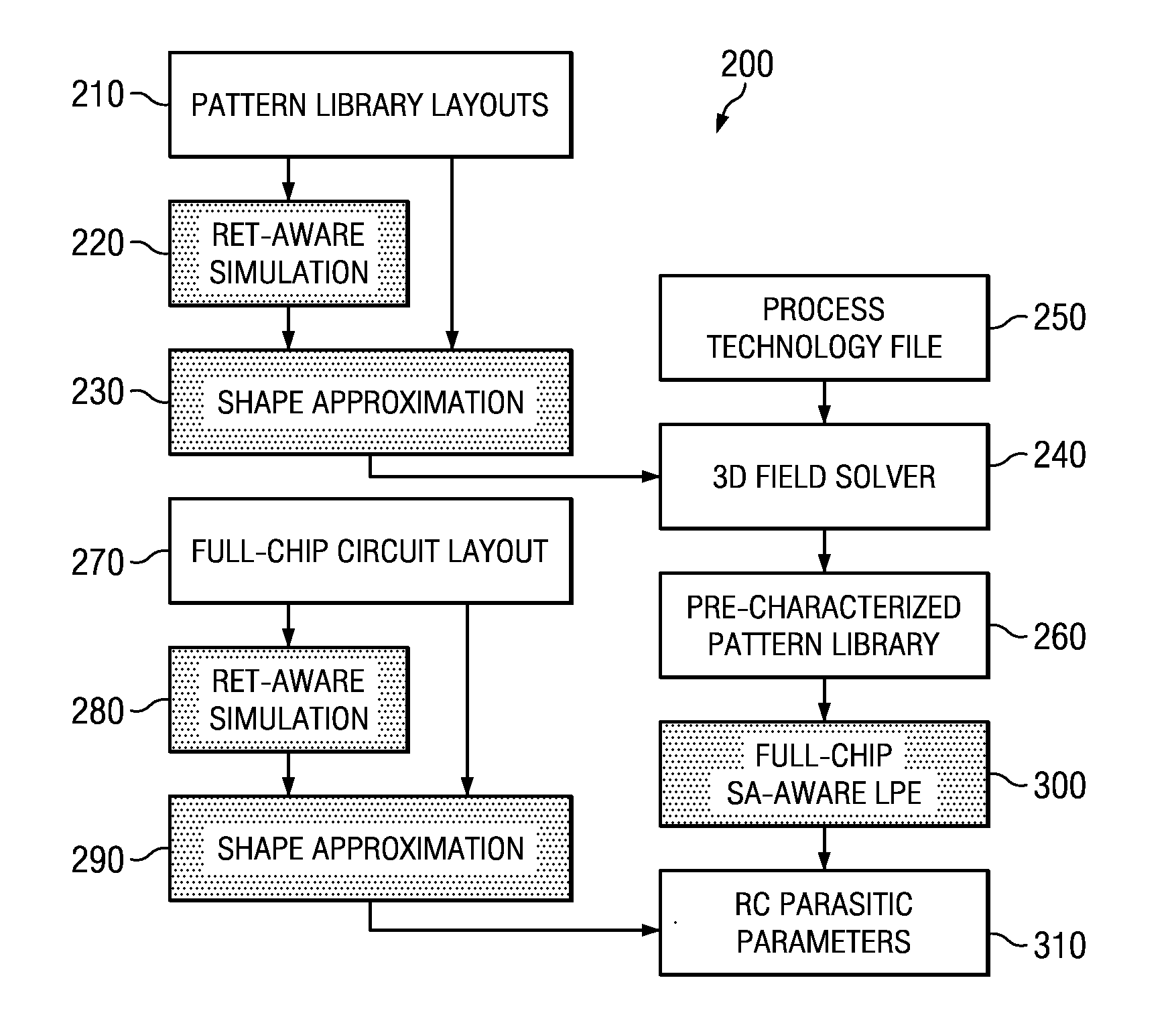
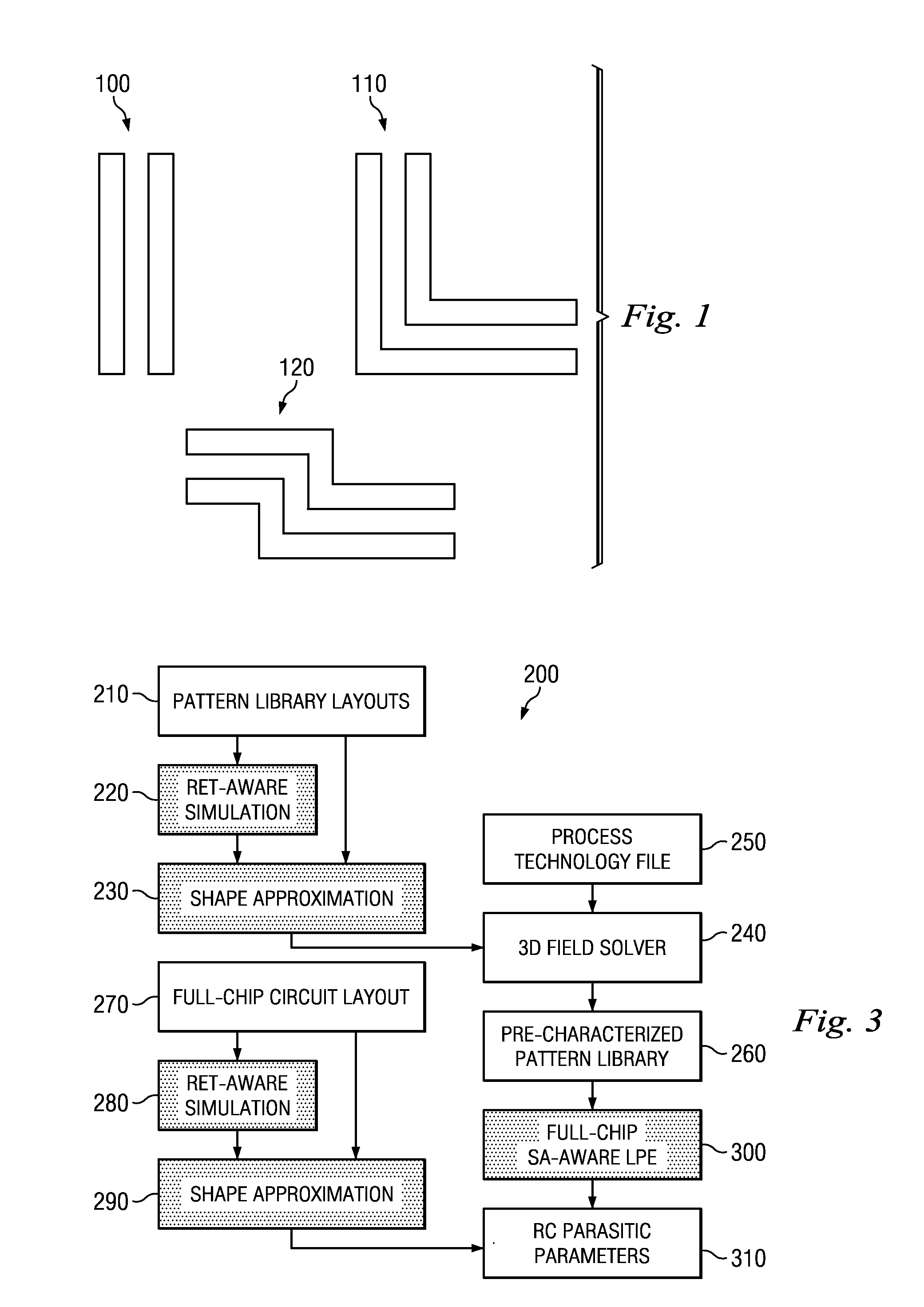
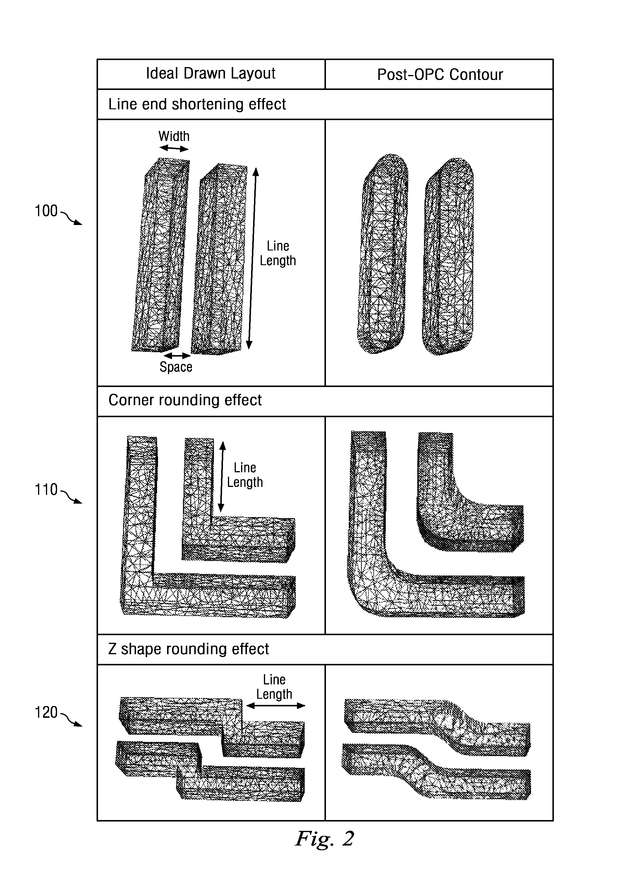
[0019]Proper electrical performances of integrated circuits depend on effective dimension control by manufacturing. The shape of integrated circuits is primarily determined by patterning fidelity of lithography processes. Due to diffraction, the minimum half-pitch resolvable for optical projection lithography is described by the Rayleigh equation k1*λ / NA, wher...


PUM


Abstract

The present disclosure involves a method. The method includes decomposing a layout of a circuit into a plurality of patterns. The method includes generating a plurality of contours to represent the plurality of patterns after the patterns have been subjected to a manufacturing process. The method includes generating a plurality of polygons that approximate geometries of the contours, respectively. The method includes associating each of the polygons with a respective one of a plurality of pattern elements in a pattern library, wherein the pattern elements each include a shape that resembles the associated polygon and electrical parameters extracted from the shape. The method includes calculating electrical performance of the circuit based on the pattern elements associated with the polygons.

Description

PRIORITY DATA[0001]This application claims priority to Provisional Application Ser. No. 61 / 434,050, filed on Jan. 21, 2011, entitled “METHOD FOR IMPROVING ACCURACY OF PARASITICS EXTRACTION CONSIDERING SUB-WAVELENGTH LITHOGRAPHY EFFECTS,” the entire disclosure of which is incorporated herein by reference.BACKGROUND[0002]The semiconductor integrated circuit (IC) industry has experienced rapid growth in recent years. Technological advances in IC materials and design have produced generations of ICs where each generation has smaller and more complex circuits than the previous generation. However, these advances have increased the complexity of processing and manufacturing ICs and, for these advances to be realized, similar developments in IC processing and manufacturing are needed. In the course of IC evolution, functional density (i.e., the number of interconnected devices per chip area) has generally increased while geometry size (i.e., the smallest component that can be created using...

Claims


Application Information

Patent Timeline
Patent Type & Authority Applications(United States)
IPC IPC(8): G06F17/50
CPCG06F2217/12G06F17/5081G06F30/398G06F2119/18Y02P90/02
Inventor TSAI, KUEN-YUHSIEH, WEI-JHIHCHANG, BO-SEN
Owner TAIWAN SEMICON MFG CO LTD
Why Eureka
Try Eureka