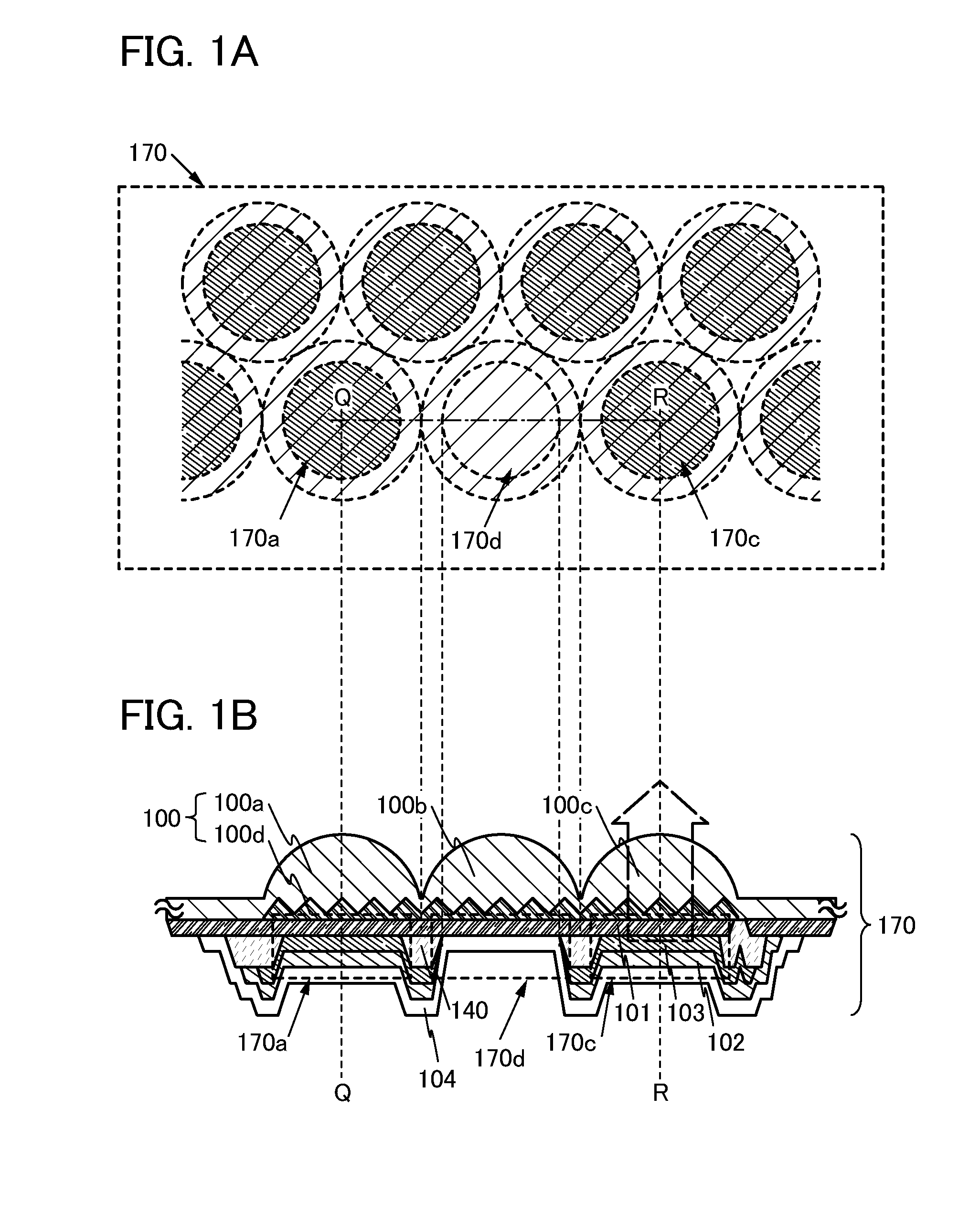
[0012]In order to achieve the above objects, the present invention focuses on a hemispherical lens which is provided to overlap with a light-emitting region of a light-emitting element to increase extraction efficiency of light.
[0016]The above embodiments of the present invention are a method in which a defective portion of a light-emitting device including a light-emitting element and a hemispherical lens overlapping with a light extraction region of the light-emitting element is insulated by
irradiation with a laser beam through the hemispherical lens. According to this method, a light-emitting device can be manufactured by insulation of a defective portion of a light-emitting element included in the light-emitting device. In addition, the above embodiments of the present invention are a method in which the hemispherical lens disposed close to the defective portion is used to condense
laser beams. According to this method, an optical
system having a
high magnification and a narrow
depth of focus are not needed to be disposed close to a surface to be irradiated, whereby the structure of a manufacturing apparatus can be simplified. Moreover, the above embodiments of the present invention are a method in which the hemispherical lens is disposed between the defective portion and a laser
irradiation unit so that the defective portion is irradiated with a laser beam. According to this method, an evaporated material from the surface to be irradiated does not contaminate the laser
irradiation unit and thus the frequency of maintenance can be reduced.
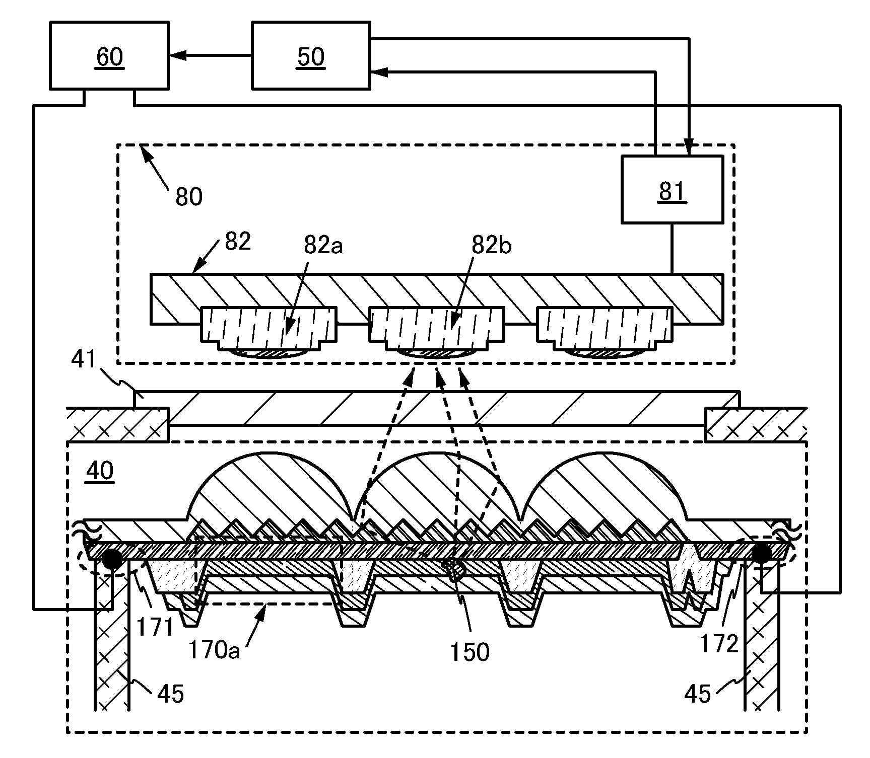
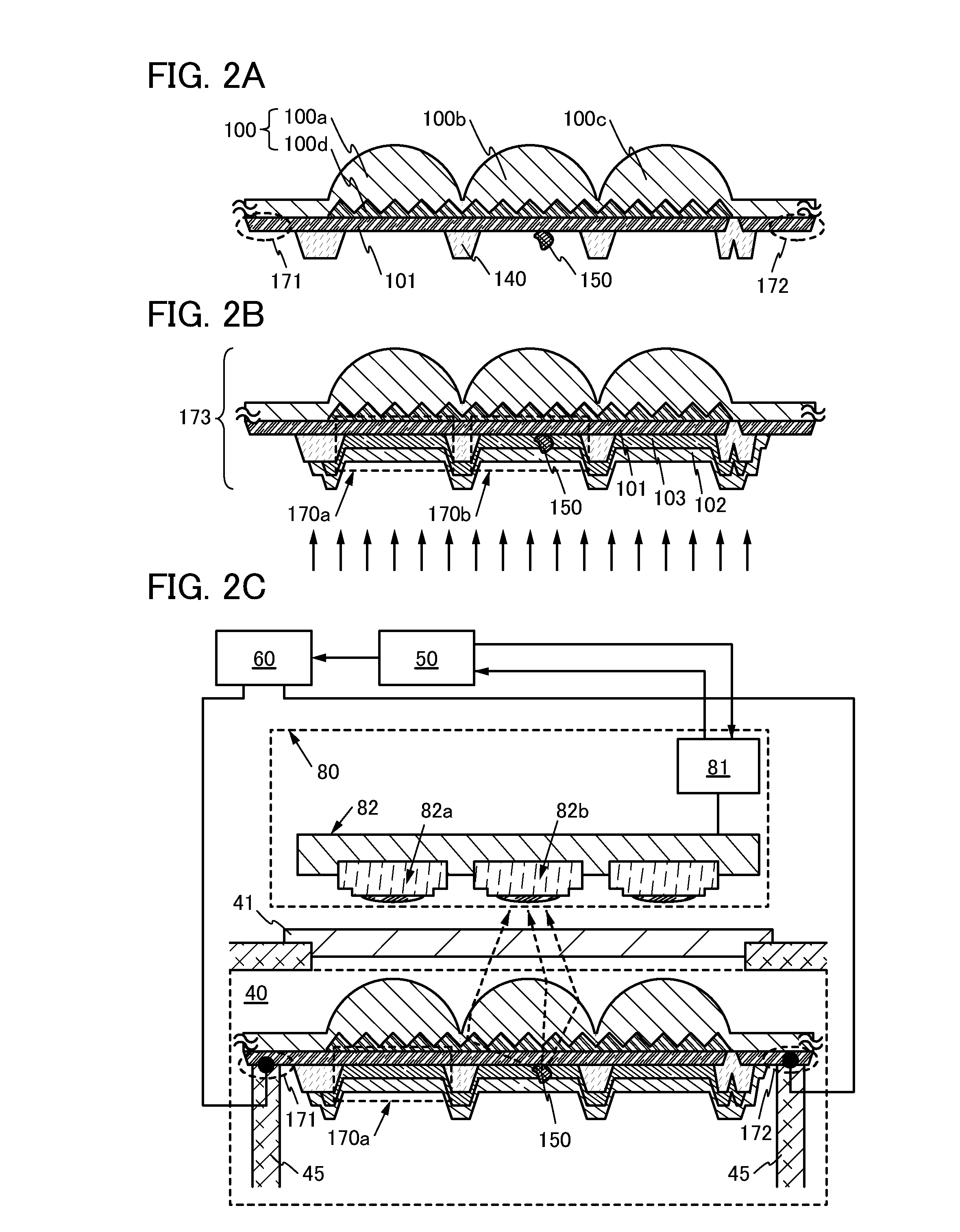
[0018]The above embodiment of the present invention is a method in which a substrate with a light-emitting element is disposed in a treatment chamber where the pressure is reduced; a defective portion of the light-emitting element, which overlaps with a light extraction region of the light-emitting element, is detected; and the defective portion is insulated by irradiation with a laser beam through a hemispherical lens and a window material provided on a wall surface of the treatment chamber, which transmits the laser beam. According to this method, a light-emitting device can be manufactured by insulation of a defective portion of a light-emitting element provided in a substrate with a light-emitting element before a sealing member is provided. In addition, the above embodiment of the present invention is a method in which the hemispherical lens disposed close to the defective portion is used to perform insulation by condensed
laser beams. According to this method, an optical
system having a
high magnification and a narrow
depth of focus are not needed to be disposed, whereby the structure of a manufacturing apparatus can be simplified. Moreover, the above embodiment of the present invention is a method in which the hemispherical lens is disposed between the defective portion and a laser irradiation unit so that the defective portion is irradiated with a laser beam. According to this method, an evaporated material from the surface to be irradiated does not contaminate the laser irradiation unit and thus the frequency of maintenance can be reduced.
[0020]The above embodiment of the present invention is a method for manufacturing a light-emitting device, in which a laser beam whose
energy density is relatively low is condensed to a defective portion of a light-emitting element with a hemispherical lens and the defective portion is insulated. According to this method, a laser whose output is relatively small can be used, whereby the cost of an apparatus can be reduced. Moreover, with the use of a laser irradiation unit in which a plurality of lasers whose output is relatively small and which is inexpensive is arranged,
processing can be performed in parallel. Further, with the use of a plurality of generated
laser beams whose
energy density is low by
divergence from a laser beam whose energy density is high,
processing can be performed in parallel. When the
processing can be performed in parallel, the processing time can be shortened as an advantageous effect.
[0022]The above embodiment of the present invention is a method for manufacturing a light-emitting device, in which a
reverse bias voltage is applied to a light-emitting element, current is made to flow through a defective portion which is a defect of a
short circuit between a pair of electrodes or a potential defect, and the defective portion is detected. According to this method, current unlikely flows through a normal portion of the light-emitting element but flows through the defective portion; therefore, the defective portion can be detected easily. Further, light emitted from the defective portion can be extracted at high efficiency from the unit for detecting a defective portion side by the hemispherical lens; therefore, the defective portion can be detected easily. Specifically, near-
infrared light emitted from the defective portion can be extracted at high efficiency. Furthermore, the following failures can be prevented: a failure in which
high current is made to flow without intention through a defective portion by application of a forward bias
voltage to a light-emitting device including the defective portion, which results in destroy of the light-emitting element including the defective portion; and a failure in which a normal light-emitting element adjacent to the light-emitting element including the defective portion or even the entire light-emitting device is destroyed.
[0024]The above embodiment of the present invention includes an evacuation unit, and, inside a treatment chamber separated from the air, a unit for supporting a substrate with a light-emitting element, in which a hemispherical lens overlapping with a light extraction region of the light-emitting element is provided, to face a window material provided on a wall surface of the treatment chamber. In addition, outside the treatment chamber, the following are included: a power supply which outputs a potential for detecting a defective portion (e.g., a
reverse bias potential) to the light-emitting element; a unit for detecting a defective portion which can detect near-
infrared light caused by current flowing through the defective portion and which includes a near-
infrared sensor capable of generating an image including positional information of the defective portion; a laser irradiation unit which emits a laser beam with which the defective portion can be irradiated; and a
control unit. According to this structure, a light-emitting device can be manufactured by insulation of the defective portion of the light-emitting element provided in the substrate with the light-emitting element before a sealing member is provided. Moreover, an evaporated material from a surface to be irradiated does not contaminate the laser irradiation unit and thus the frequency of maintenance can be reduced. Further, a unit for forming a sealing member is included in addition to the above structure. According to this structure, after the defective portion is insulated, a sealing member covering the insulated portion can be formed. Since the sealing member can be formed directly on the insulated portion, a phenomenon in which an
impurity is diffused into the light-emitting element from the insulated portion can be prevented.

