Integrated semiconductor solar cell package

a solar cell and integrated technology, applied in the field of semiconductor photovoltaic device packaging, can solve the problems of high mechanical failure rate in actual use, photovoltaic devices, current solar cell package designs, etc., and achieve the effects of less expensive, convenient and convenient manufacturing, and less energy consumption

Active Publication Date: 2012-08-09
CACTUS MATERIALS INC
View PDF8 Cites 6 Cited by
  • Summary
  • Abstract
  • Description
  • Claims
  • Application Information

AI Technical Summary

Benefits of technology

[0007]According to the invention, a stacked component solar cell package is provided that has a planar arrangement of conductive laminates at or below the surface of a heat sink in order to isolate the solar cell electrically from the heat sink. The present invention provides durable and easily manufactured solar chip packages with lower vertical and narrower horizontal profiles, presenting a more versatile package and a less expensive manufacturing alternative to current chip packaging technologies. The described invention further allows for electrical connections to be made between the chip and a protective bypass diode or other external circuitry without the need for complex, time consuming, expensive, and vulnerable plastic packaging and soldered interconnections.
[0008]The planar alignment allows more electrical connections below the surface of the heat sink, twice as many as known current solar packages. This layout also reduces the vertical profile of the solar package, allowing it to be more easily sealed (against moisture or hemietically) with the primary and secondary optics.
[0009]Also according to the invention, a stacked component solar cell package is provided having one or more thermally-conductive laminates integrated with the heat sink. These conductive laminates comprise non-ceramic PCB-board type materials, allowing more efficient and cost-effective heat dissipation, and eliminate the need for a thermally conductive substrate layer (typically ALN or BeO) between the solar cell and the heat sink. These embodiments allow electrical connections to be made between the chip and a protective bypass diode or other external circuitry without the need for complex, time consuming, expensive, and vulnerable plastic packaged devices. An additional benefit is that the substrate can be embedded within the heat sink during the manufacturing phase, simplifying the assembly process and making assembly of the solar package faster, less expensive, and more easily scalable.
[0010]Packaging as described permits the use of standard photovoltaic semiconductor chips having an anode on one surface and a cathode on the other without the need for expensive processing of the chip, extra masks or custom assembly equipment. Use of the invention simplifies the assembly of the solar cell components, both as to the package itself and later for subassembly and connectivity requirements. The package design also allows for scaling the manufacturing process to high volume output in a relatively short time. Additionally, the design allows the solar package to be downsized to ultimately reduce the size of commercial solar arrays. Other benefits from the invention will become readily apparent to those of skill in the arts of semiconductor design and packaging from the following detailed description in connection with the accompanying drawings.

Problems solved by technology

Photovoltaic devices present unique problems requiring specialized packaging to achieve desired levels of durability, mechanical integrity, electrical connectivity, maximum thermal transfer, and convenience of mounting.
The delicate semiconductor material used as the operative portion of a solar cell must be protected from excessive current by attaching, for example, an additional device such as a bypass diode in parallel with the anode and cathode of the device, an operation nomially accomplished by soldering surface mount plastic packaged devices in a manner that may cause high rates of mechanical failure in actual usage.
Current solar cell package designs suffer from design and component limitations that restrict package usage.
Because of the limited number of suppliers, use of these ceramic substrates increases the cost of manufacturing the solar packaging.
Commercialized solar packages also require that the chip, thermally conductive substrates, and heat sink be stacked vertically, increasing the profile of the package and thereby making hermetic sealing of the solar package more difficult and expensive.
A further limitation of solar packaging designs in current use is a maximum platform size of 4.5 inches×4.5 inches.

Method used


Image

  • Integrated semiconductor solar cell package
  • Integrated semiconductor solar cell package
  • Integrated semiconductor solar cell package

Examples


Embodiment Construction

Substrate Insert Embodiments

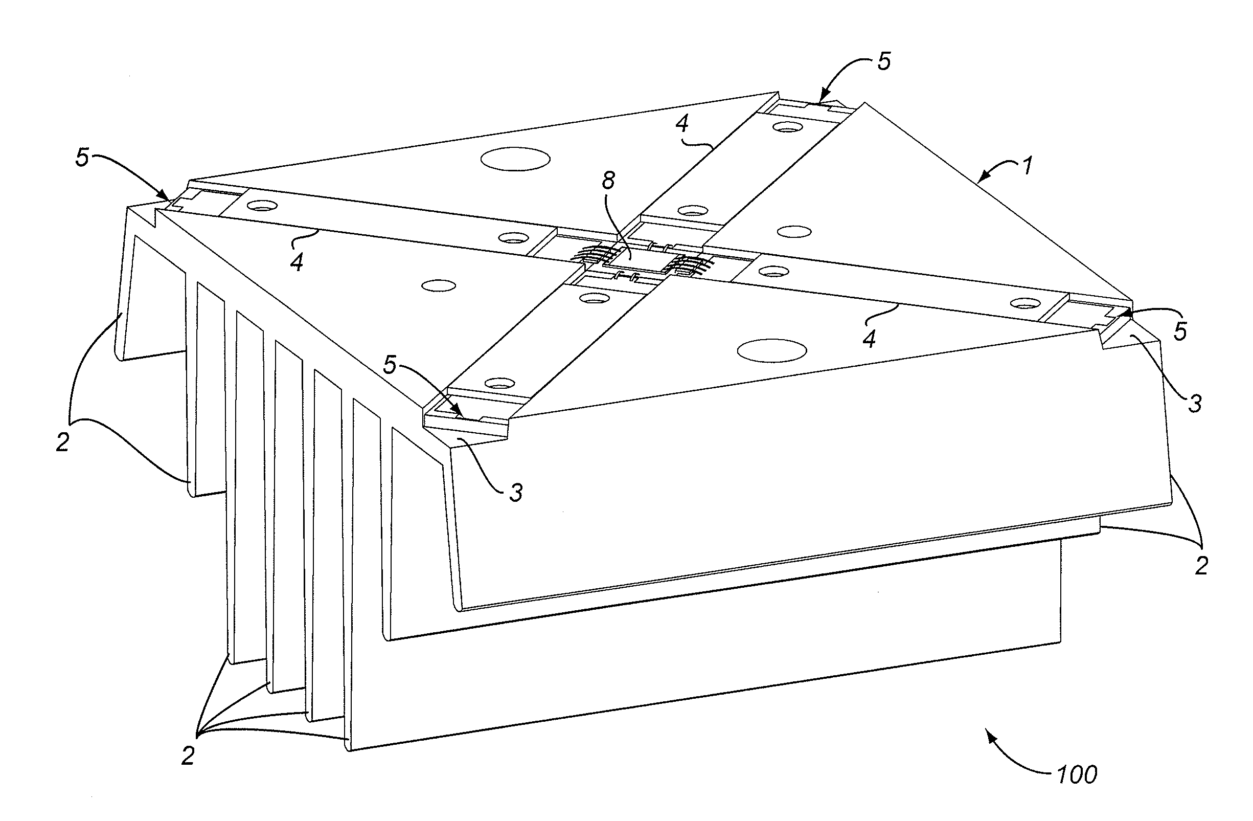
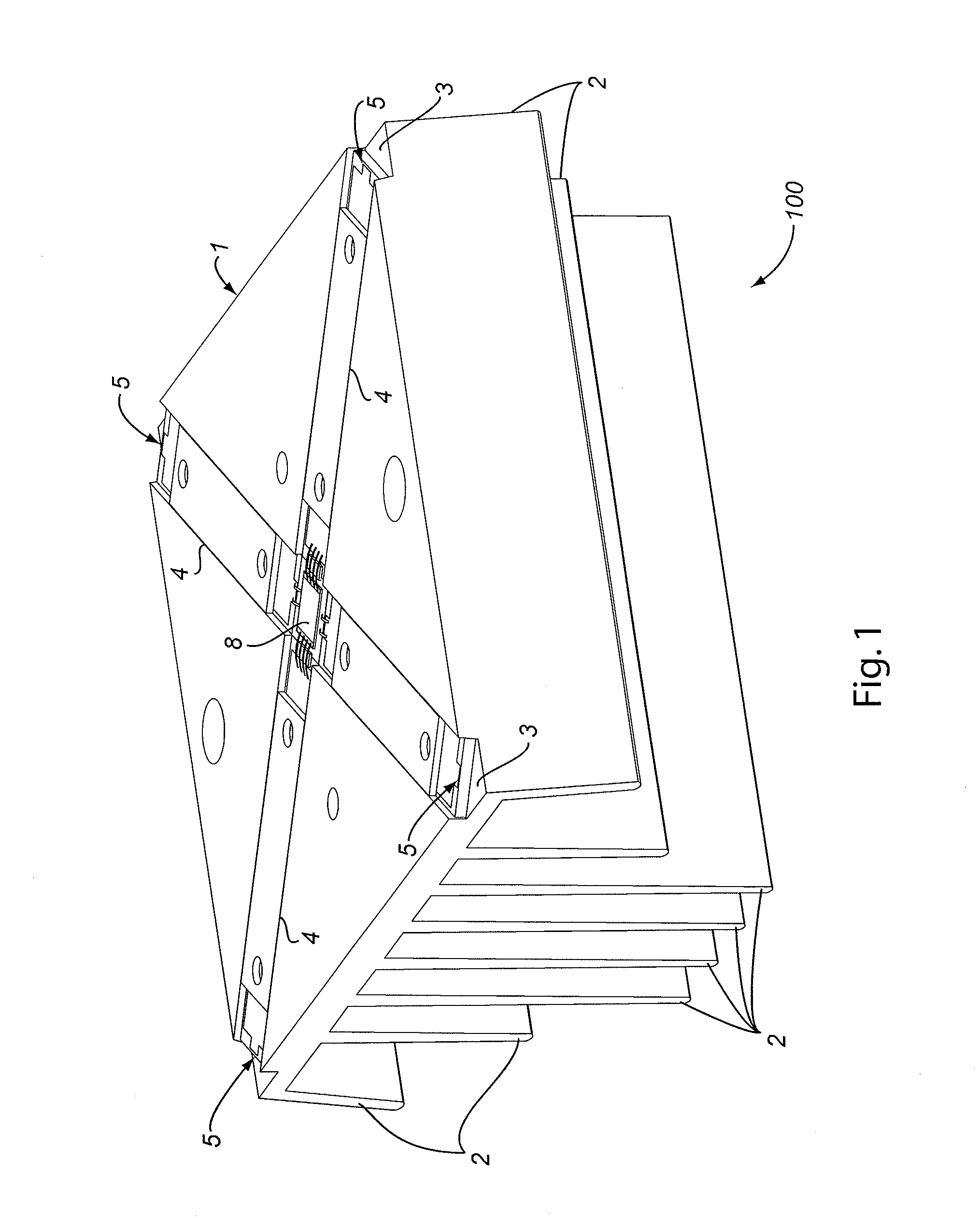
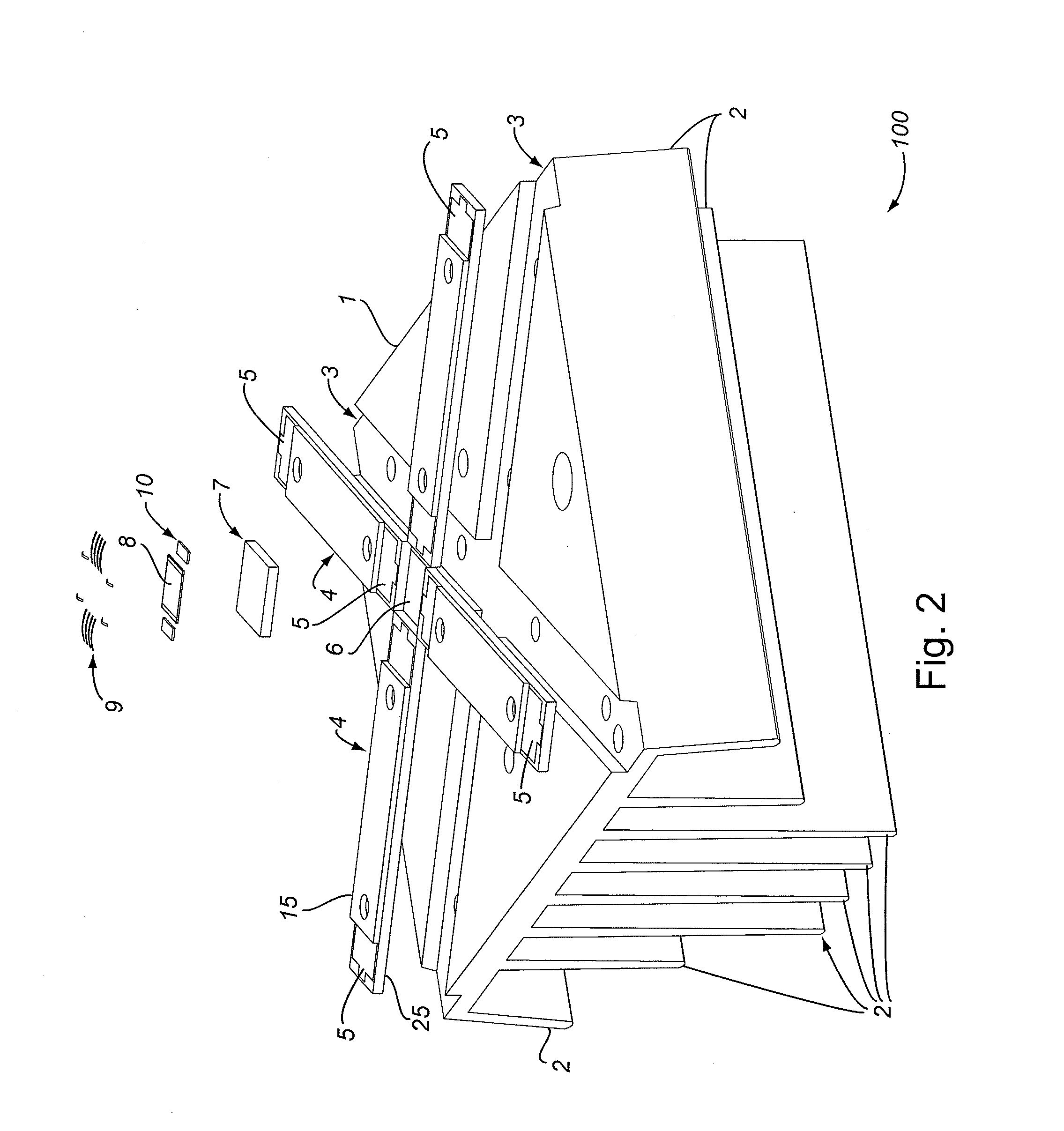
[0025]FIG. 1 shows one embodiment of a completed solar cell package assembled from the various stackable components as shown in FIG. 2. The solar cell package includes five components: a multi junction solar chip, bypass diodes, a substrate insert, four conductive laminates, and a heat sink. The solar chip in this embodiment is a III-V multi junction solar cell, but the structure is compatible with other planar chips with any semiconductor material that must be exposed to weather and a wide range of thermal expansion and contraction.

[0026]Referring to FIGS. 2 and 5, the lowest level of the package is a metal base used as a master heat sink 1. The base is preferably aluminum, but any metal or metallic alloy that is machinable or castable will suffice. The base in this embodiment is a modified flat top heat sink with cooling fins of the sort commercially available (e.g., from AAVID Thermalloy LLC of Concord, N.H.). Several cooling fins 2 protrude from the b...


PUM


Abstract

A stacked package for a solar cell is provided with a planar arrangement of conductive laminates on the surface of the heat sink. The layered conductive laminate offers multi-directional orientation of the solar cell within the package by eliminating any orientation requirements between the chip and the substrate, and offers multiple options for placement of standard or flipped bypass diodes. The packaged solar cell of the invention provides a smaller horizontal and vertical profile than standard solar cell packages, making it easier to hermetically seal the package.

Description

CROSS-REFERENCES TO RELATED APPLICATIONS[0001]The present application claims benefit under 35 USC 119(e) of U.S. provisional Application No. 61 / 439,082 filed on Feb. 3, 2011, entitled “Integrated Semiconductor Solar Cell Package,” and U.S. provisional Application No. 61 / 439,095 filed on Feb. 3, 2011, entitled “Flexible Hermetic Semiconductor Solar Cell Package With Non-Hermetic Option,” the contents of which are incorporated herein by reference in their entirety.STATEMENT AS TO RIGHTS TO INVENTIONS MADE UNDER FEDERALLY SPONSORED RESEARCH OR DEVELOPMENT[0002]NOT APPLICABLEREFERENCE TO A “SEQUENCE LISTING,” A TABLE, OR A COMPUTER PROGRAM LISTING APPENDIX SUBMITTED ON A COMPACT DISK[0003]NOT APPLICABLEBACKGROUND OF THE INVENTION[0004]This invention relates to packaging for semiconductor photovoltaic devices known generally as solar cells.[0005]Photovoltaic devices present unique problems requiring specialized packaging to achieve desired levels of durability, mechanical integrity, elec...

Claims


Application Information

Patent Timeline
Patent Type & Authority Applications(United States)
IPC IPC(8): H01L31/024H01L31/0203
CPCY02E10/50H01L31/052H01L31/02008
Inventor LAMARCHE, PAUL F.
Owner CACTUS MATERIALS INC
Why Eureka
Try Eureka