
Wiring substrate and method of manufacturing the same

a wiring substrate and manufacturing method technology, applied in the direction of superimposed coating process, printed circuit aspects, coatings, etc., can solve the problems of affecting the application of such a wiring substrate to desired high-frequency applications, affecting the effect of preventing deterioration of high-frequency characteristics, and affecting the adhesion reliability. to achieve good high-frequency characteristics, improve the effect of adhesion reliability, and simplify the surface modification step

Inactive Publication Date: 2012-08-16
NGK SPARK PLUG CO LTD
View PDF6 Cites 14 Cited by
  • Summary
  • Abstract
  • Description
  • Claims
  • Application Information

AI Technical Summary

Benefits of technology

[0009]According to the wiring substrate of the present invention, of the conductor layers of the laminate portion, each of the conductor layers other than the signal line layer has a roughened surface treated with a roughening treatment, and the signal line layer has a flat surface treated with a surface modification treatment rather than the roughening treatment. This structure provides advantageous effects. That is, in the laminate portion composed of the insulating layers and the conductor layers, a roughening treatment is performed on the conductor layers other than the signal line layer. Thus, adhesion is secured between the conductor layers and the insulating layers by the anchor effect of protrusions and depressions on the surfaces of the conductor layers. In addition, through performance of a proper surface modification treatment on the signal line layer, adhesion between the surface of the signal line layer and the adjacent insulating layer is secured through chemical bonding between the surface of the signal line layer and the insulating layer. Therefore, it is possible to prevent occurrence of deficiencies such as surface bulging or separation of each conductor layer, which would otherwise occur when the wiring substrate is heated. Also, even in the case where the signal line layer has a conductor pattern for high-frequency signals, current concentrates at the flat conductor surface having no uneven portion (protrusions and depressions) due to the skin effect. Therefore, conductor loss can be reduced, and satisfactory high-frequency characteristics can be maintained.
[0010]A typical example of the surface modification treatment performed on the signal line layer is a silane coupling treatment performed through use of a silane coupling agent. The silane coupling agent is an organic silane compound having an organic functional group which reacts with an organic substance. When the silane coupling treatment is performed on the signal line layer, the silane coupling agent is applied to the surface of the signal line layer to a predetermined thickness, and a resin is applied onto the signal line layer in this state. As a result, the organic functional group of the silane coupling agent reacts with the organic functional group of the resin material, whereby chemical coupling is produced on the conductor surface, and the conductor surface is modified. Thus, the signal line layer and the adjacent insulating layer can be bonded at the interface therebetween. No particular limitation is imposed on a method of preparing the silane coupling agent and additives thereof, and the preparation method and additives can be properly selected in accordance with treatment conditions.
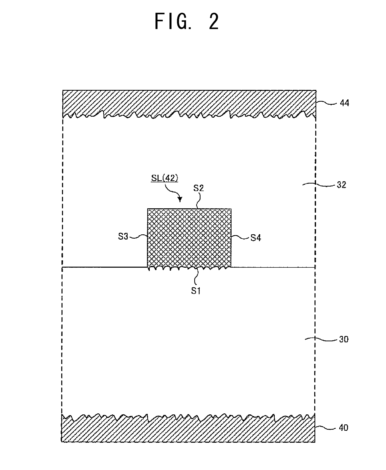
[0011]The signal line layer can be formed to have any of various configurations. For example, as viewed in a cross section of the signal line layer taken along a thickness direction thereof, a surface of the signal line layer in contact with an insulating layer which is adjacently located on one side (i.e., a first side) of the signal line layer is not the flat surface, and a surface of the signal line layer in contact with an insulating layer which is adjacently located on the other side (i.e., a second side) of the signal line layer is the flat surface. In this case, an example of a surface which is made flat includes a surface of the signal line layer that is in contact with an insulating layer adjacent to the signal line layer. The surface may include opposite side surfaces of each conductor trace of the signal line layer. Thus, even though one of the surfaces (generally, of four side surfaces) of each conductor trace through which a high-frequency signal is to be transmitted is a roughened surface, the remaining surfaces are treated with a surface modification treatment. Therefore, it is possible to simplify the surface modification step in a wiring substrate manufacturing process, without impairing the effect of preventing deterioration of high-frequency characteristics, which would otherwise occur due to the skin effect.
[0012]Although no particular limitations are imposed on the dimensional conditions of the signal line layer, preferably, the surface roughness Ra of the flat surface is set to be less than 0.1 μm, and the surface roughness Ra of the roughened surface of each of the conductor layers other than the signal line layer is set to 0.1 μm or greater. In this case, the surface roughness Ra of the flat surface is desirably set to such a value that the surface roughness Ra can be substantially considered to be 0 μm.
[0013]In the wiring substrate of the present invention, the insulating layers adjacent to the signal line layer may be formed through use of a material which is smaller in relative dielectric constant than the remaining insulating layer(s). By virtue of this configuration, high-frequency signals are transmitted through signal lines in a state in which a material which is low in dielectric constant and which has good high-frequency characteristics is disposed around the signal lines. Together with the effect of the surface modification treatment, use of such a material further improves the high-frequency characteristics. Notably, the same effect can be expected even in the case where not only the relative dielectric constant of the material of the insulating layers, but also the tan δ (electric loss tangent) of the material of the insulating layers is decreased.
[0014]The wiring substrate of the present invention can be formed to have any of various configurations. For example, the wiring substrate may include a substrate core and be configured such that the laminate portion is formed on each of opposite sides of the substrate core; and first and second signal line layers disposed in the respective laminate portions, wherein the substrate core intervenes between the first and second signal line layers. For example, a first signal line layer may be formed at a predetermined layer position of the laminate portion located on one side of the substrate core, and a second signal line layer may be formed at a predetermined layer position of the laminate portion located on the other side of the substrate core such that the second signal line layer becomes symmetric with the first signal line.

Problems solved by technology

In the case where a roughening treatment is performed on the surface of such a conductor layer as described above, because of the skin effect, current flows intensively through the uneven portion at the surface of the conductor, whereby conductor loss increases significantly.
Thus, transmission characteristics associated with transmission of high-frequency signals through the wiring substrate deteriorate, which hinders application of such a wiring substrate to desired high-frequency applications.
However, in such a case, adhesion reliability cannot be secured, and occurrence of defects during manufacture cannot be avoided.
Therefore, such measure is not realistic.
As described above, the conventional wiring substrate structure has a problem in that securement of satisfactory high-frequency characteristics associated with transmission of high-frequency signals and securement of adhesion reliability at the time of manufacture cannot be realized simultaneously.

Method used


Image

  • Wiring substrate and method of manufacturing the same
  • Wiring substrate and method of manufacturing the same
  • Wiring substrate and method of manufacturing the same

Examples


first embodiment

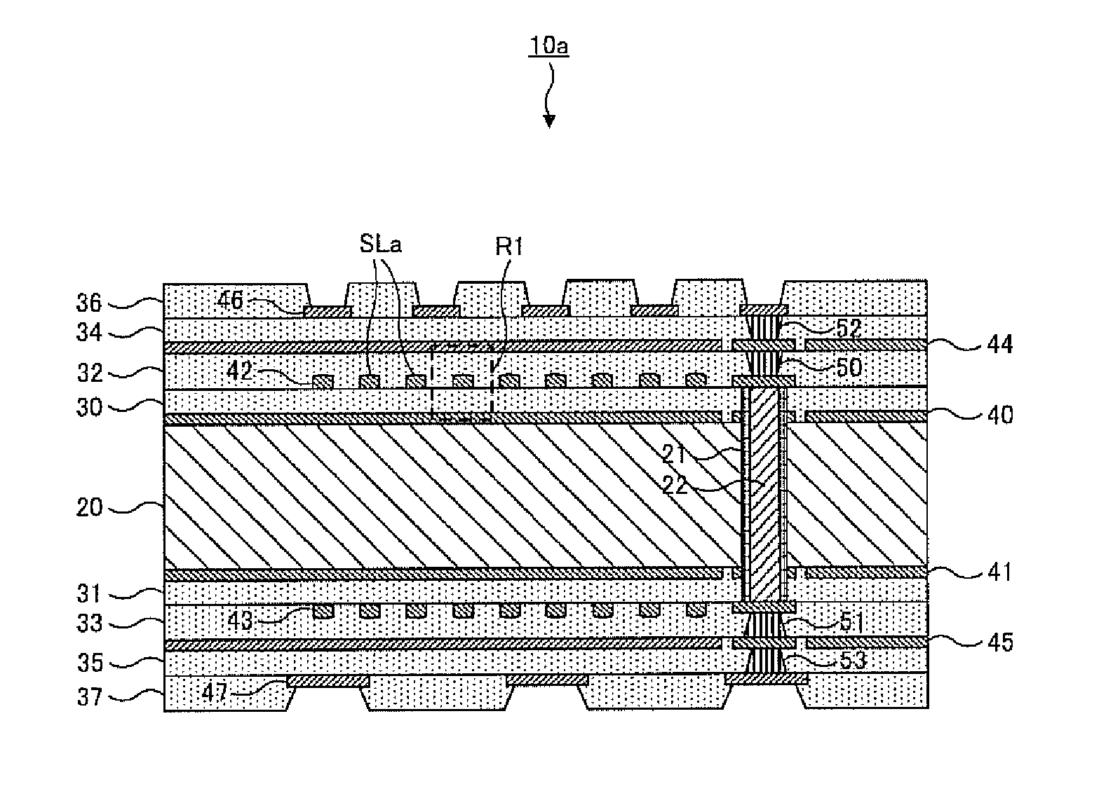
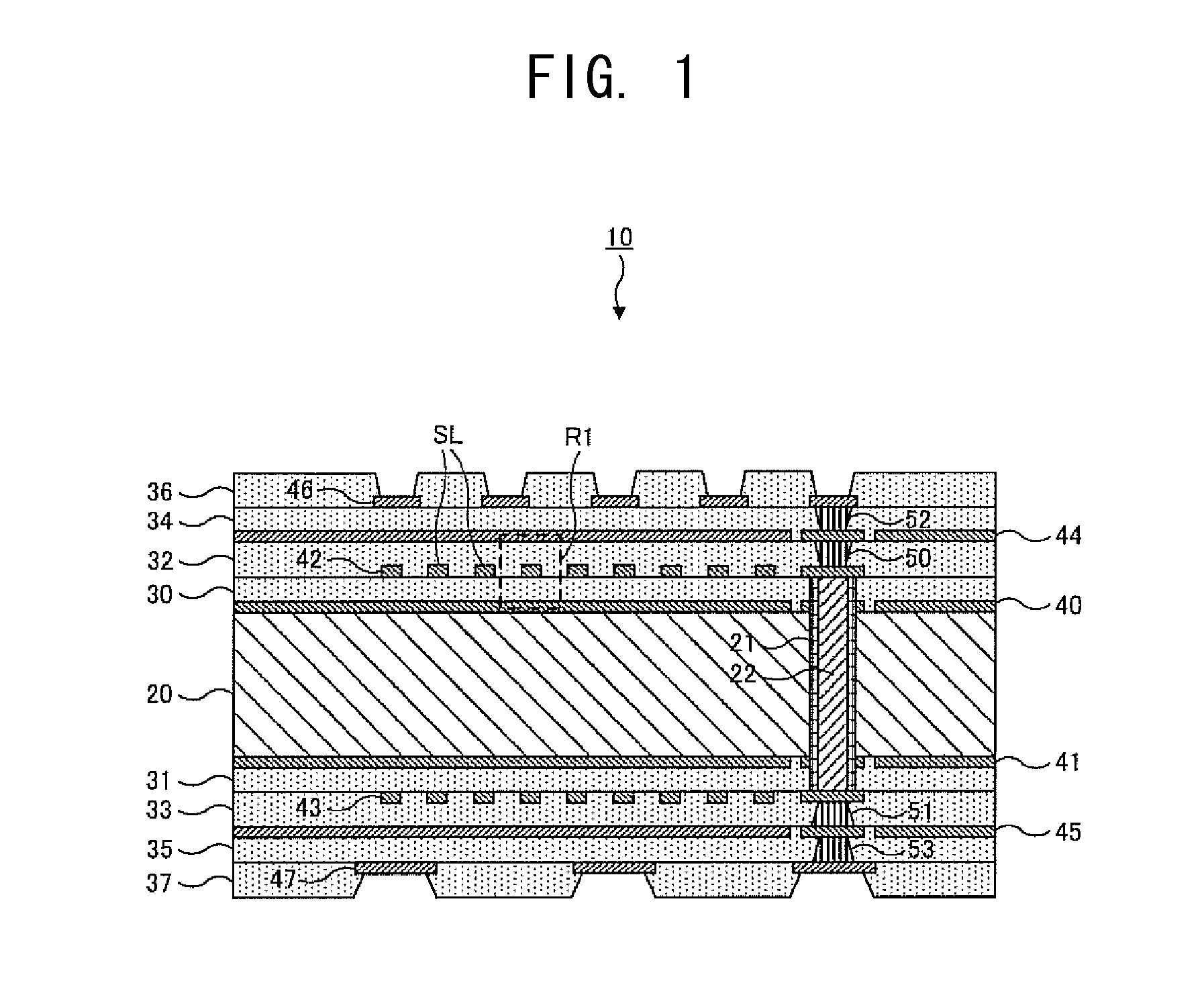
[0039]A signal line layer 42, which is a conductor layer, is formed on the surface of the insulating layer 30. This signal line layer 42 includes a large number of signal lines SL for transmitting high-frequency signals. Also, a signal line layer 43, which is a conductor layer, is formed on the surface of the insulating layer 31. This signal line layer 43 has the same structure as the above-described signal line layer 42. The upper end and lower end of the through hole conductor 21 are connected to conductor traces of the signal line layers 42 and 43, respectively. The wiring substrate 10 of the first embodiment is characterized in that, in order to attain satisfactory high-frequency characteristics and satisfactory adhesion reliability, a silane coupling treatment is performed on the signal line layers 42 and 43 so as to form flat surfaces. The specific structure and action of the signal line layers 42 and 43 will be described later.

[0040]A conductor layer 44 is formed on the surfa...

second embodiment

[0063]Since the signal line SLa has a curve cross-sectional shape such that the top surface S2a of the signal line SLa projects upward as shown in FIG. 13, concentration of stress at a corner portion of the signal line SLa can be mitigated. That is, the signal line SLa, which is formed of a metallic material, is surrounded by the insulating layers 30, 32 formed of a resin material, and thermal stress acts on the signal line SLa due to a difference in coefficient of thermal expansion therebetween. Since this thermal stress concentrates on corner portions of the cross-sectional structure of the signal line SLa where the top surface S2a perpendicularly intersects the side surfaces S3, S4, resin cracking may occur near the corner portions. In the second embodiment, the top surface S2a having a convex cross section is formed in a plating step to be described later, whereby opposite corner portions have obtuse angles greater than a right angle, to thereby mitigate concentration of stress ...


PUM

PropertyMeasurementUnit
surface roughnessaaaaaaaaaa
surface roughness Raaaaaaaaaaa
surface roughnessaaaaaaaaaa

Abstract

A wiring substrate is configured such that each of laminate portions provided above and below a substrate core includes insulating layers and conductor layers stacked alternately. Of the conductor layers of the laminate portions, signal line layers are treated with a silane coupling treatment, which is a surface modification treatment, so that each signal line comprises a flat surface. A roughening treatment is performed on the remaining conductor layers of the laminate portions such that the surfaces of these layers are roughened. This structure provides an advantage when high-frequency signals are transmitted through the signal line layers. That is, when each signal line comprises a flat surface, an increase in conductor loss due to the skin effect can be prevented. In addition, by means of chemical bonding attained through the silane coupling treatment, the reliability of adhesion between the signal line layers and the insulating layer is sufficiently attained.

Description

BACKGROUND OF THE INVENTION[0001]1. Field of the Invention[0002]The present invention relates to a multi-layer wiring substrate having a laminate portion in which insulating layers and conductor layers are stacked alternately, and more particularly to a wiring substrate suitable for transmission of high-frequency signals.[0003]2. Description of Related Art[0004]Conventionally, a wiring substrate which includes a substrate core and laminate portions provided on opposite sides of the substrate core and each including insulating layers and conductor layers stacked alternately has been widely used as a package on which a semiconductor chip or the like is mounted. In a process of manufacturing a wiring substrate having such a structure, conductor layers formed of metal such as copper and insulating layers formed of resin must be stacked such that a sufficient degree of adhesion is ensured between them. If a sufficient degree of adhesion is not secured between each conductor layer and the...

Claims


Application Information

Patent Timeline
Patent Type & Authority Applications(United States)
IPC IPC(8): H05K1/02H05K3/22C23C28/00H05K3/00
CPCH05K2201/098H05K1/0242H01L23/49822H05K2201/0347H01L23/49827H05K3/389H05K3/4644H01L2924/0002Y10T29/49156H01L2924/00H05K3/46
Inventor HIGO, KAZUNAGAIGARASHI, HIDEMASAARAKAWA, MASATSUNEYAMADA, ERINASUZUKI, KENJIANDO, TOMOHITOSATO, HIRONORITORII, TAKUYA
Owner NGK SPARK PLUG CO LTD
Learn More