Device and method for transferring micro structure

a micro-structure and transfer method technology, applied in the field of micro-structure transfer devices and methods, can solve the problems of reducing the transmittance of stampers, increasing the time-consuming curing process of photo-curable resins, and low throughput of micro-structure transfer processes, and achieves excellent micro-structure transfer fidelity, good throughput, and adequate light transmittance.

Inactive Publication Date: 2012-08-16
HITACHI HIGH-TECH CORP
View PDF2 Cites 8 Cited by
  • Summary
  • Abstract
  • Description
  • Claims
  • Application Information

AI Technical Summary

Benefits of technology

[0019]The present invention provides a device and a method for transferring microstructure featuring a resin stamper with an adequate transmittance of light and an excellent fidelity of microstructure transfer, achieving a good throughput, and preventing degradation of the resin stamper.

Problems solved by technology

The increased thickness of the resin layer, however, decreases the stamper's transmittance of light, to which the photo-curable resin at the impression receptor is exposed, therefore making the curing process of the photo-curable resin more time-consuming, which means a low throughput of a microstructure transfer process.
The shorter wavelength of the passing light, however, also lowers the stamper's transmittance of the light, and inflicts a greater damage on the resin constituting the resin stamper, namely on the resin's organic functional groups.
The diminished photo energy, however, of the light, to which the photo-curable resin at the impression receptor is exposed, decreases the efficiency of the curing process of the photo-curable resin, resulting in a low throughput.
Moreover, the resin stamper having a lowered transmittance of the light due to the increased thickness of the resin layer undergoes a thermal expansion due to the photo energy of the passing light absorbed by the resin layer, which is more likely to lower precision in the image transfer or in the mask positioning.

Method used


Image

  • Device and method for transferring micro structure
  • Device and method for transferring micro structure
  • Device and method for transferring micro structure

Examples


working examples

[0132]In the following paragraphs, the present invention will be more specifically described with presentation of working examples.

working example 1

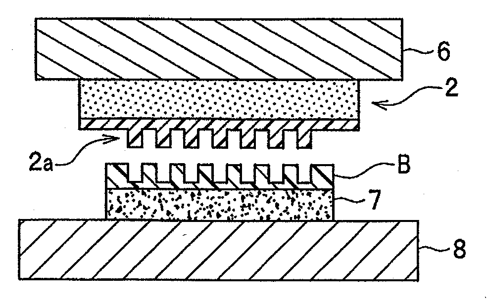
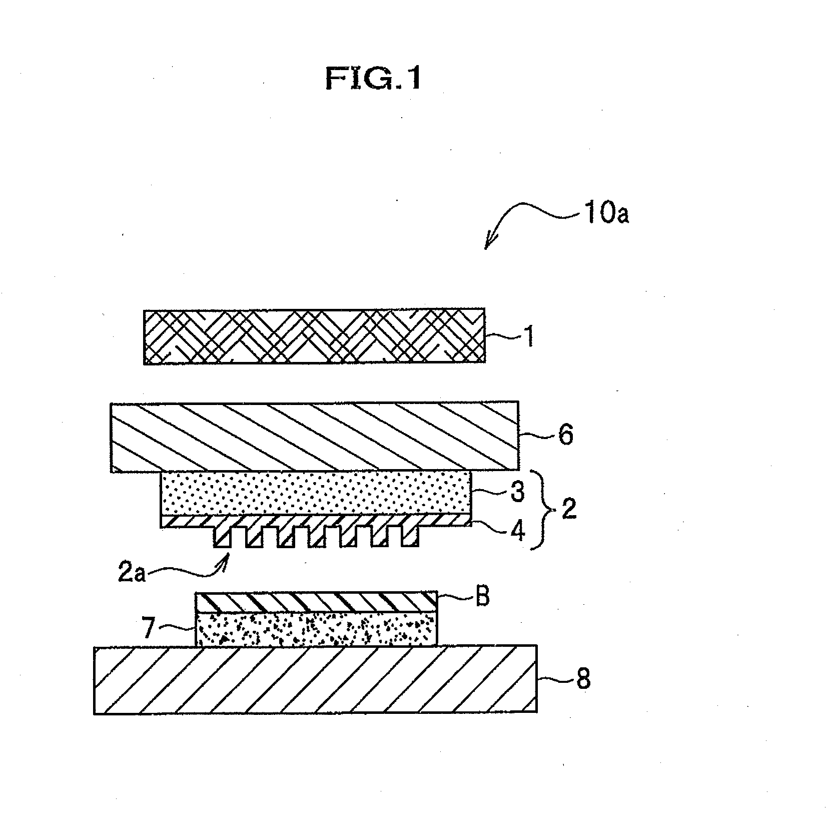
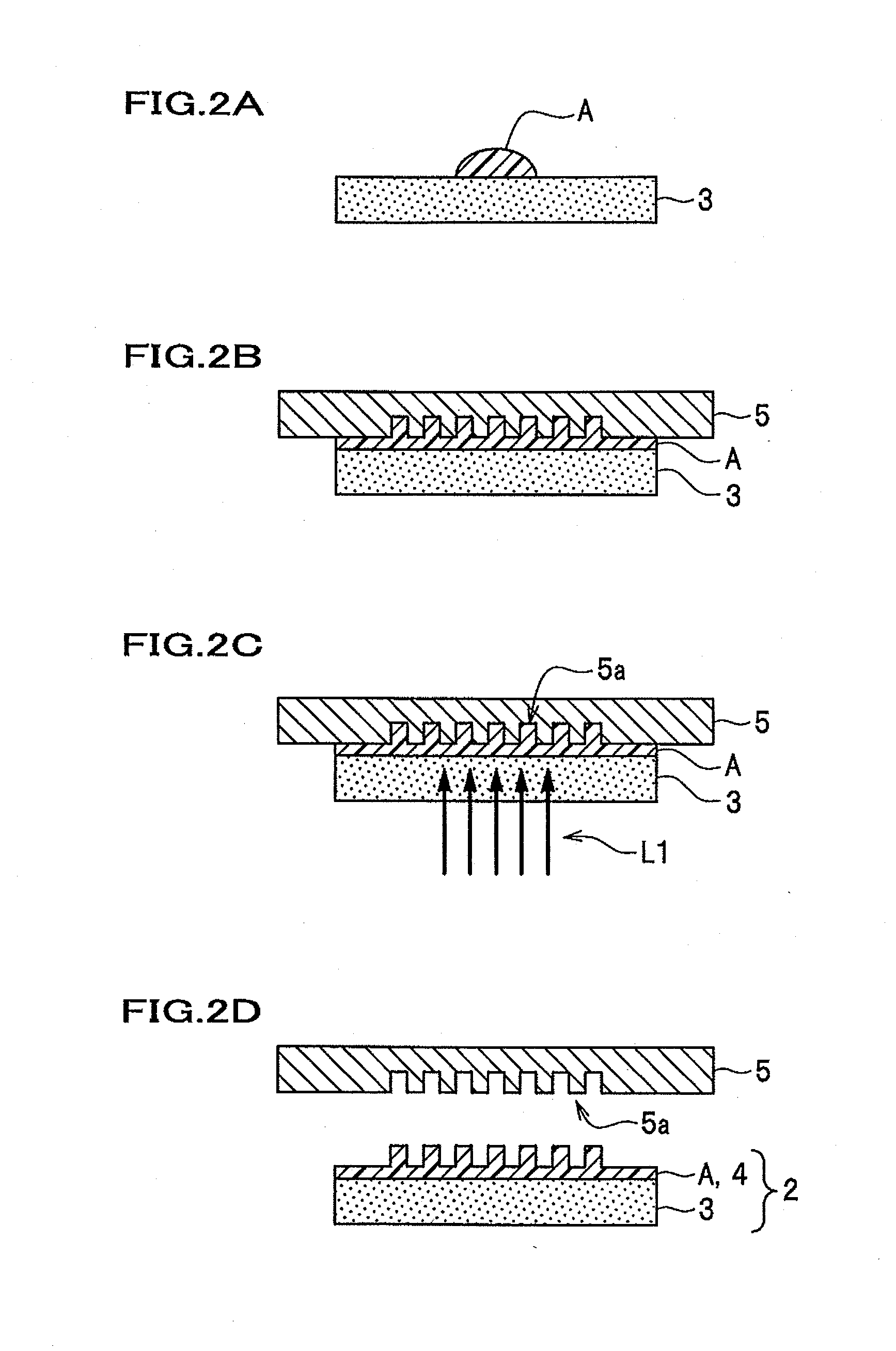
[0133]In the following working example 1, a resin stamper was formed by curing the photo-curable resin composition A (the first photo-curable resin composition) with light with the first wavelength before a microstructure-bearing body was obtained by curing, with the light L2 with the second wavelength, the photo-curable resin composition B (the second photo-curable resin composition) supplied to an impression receptor while the resin stamper was pressed against the supplied photo-curable resin B.

[0134]The prepared photo-curable resin composition A comprised 100 parts by mass of OX-SQ (a product of TOAGOSEI CO., LTD.) mixed with 5 parts by mass of ADEKAOPTOMER SP-152 (a product of ADEKA CORPORATION) as a photo-polymerization initiator A′.

[0135]A master stamper and a substrate were prepared for the formation of a resin stamper.

[0136]The master stamper bore a concentric circle pattern with a line width of 50 nm, a pitch of 100 nm, and a height of 50 nm, formed by a conventional electr...

working example 2

[0151]In Working Example 2, a microstructure was transferred to the photo-curable resin composition B in the same procedures as Working Example 1 except that the LED lamp emitting light with the wavelength of 400 nm in Working Example 1 was replaced with an LDE emitting light with a wavelength of 375 nm. As a result, a transferred microstructure, which had reversed microscopic asperities of the microstructure of the resin stamper, was recognized on the surface of the impression receptor.

[0152]In Working Example 2, a repeated use of the prepared resin stamper for 500 times on the photo-curable resin composition B produced transferred microstructures, which showed a dimensional variation of no more than ±2 nm.


PUM

PropertyMeasurementUnit
transmittanceaaaaaaaaaa
wavelengthaaaaaaaaaa

Abstract

A microstructure transferring device is characterized in that the device comprises a stamper made from a first photo-curable resin composition cured with light with a first wavelength, and a light source emitting light with a second wavelength longer than the first wavelength. The microstructure is transferred to an impression receptor supplied with a second photo-curable resin composition, which is curable with light with the second wavelength emitted by the light source.

Description

CROSS REFERENCE TO RELATED APPLICATION[0001]The present application claims priority from Japanese Patent Application No. 2011-026646 filed on Feb. 10, 2011, the disclosure of which is incorporated herein by reference.[0002]The present invention relates to a microstructure transferring device and a microstructure transferring method for forming a microstructure on a substrate.DESCRIPTION OF THE RELATED ART[0003]Conventionally the technology of photolithography is widely used as a vital technology of the micro-patterning process for a semiconductor device. As the scale of patterning becomes increasingly finer, however, the photolithography finds difficulty in meeting the requirement for a process dimension as microscopic as the scale of a wavelength of light used for exposure. In consequence, the electron beam lithography device, a kind of charged-particle-beam generator, is substituting the conventional photolithography device.[0004]Unlike the conventional one-shot exposure patternin...

Claims


Application Information

Patent Timeline
Patent Type & Authority Applications(United States)
IPC IPC(8): B29C59/16
CPCB82Y10/00B29C33/3878G03F7/0002B82Y40/00B30B15/062
Inventor WASHIYA, RYUTAOGINO, MASAHIKOSHIZAWA, NORITAKEMORI, KYOICHIMIYAUCHI, AKIHIRO
Owner HITACHI HIGH-TECH CORP
Why Eureka
Try Eureka