Spin filter device, method for its manufacture and its use

a filter device and spin filter technology, applied in the field of spin filter devices, methods for their manufacture and use, can solve the problems of difficult integration into large-scale integrated circuits or even printed circuits, inefficient for many applications, and slow internal operation

Active Publication Date: 2012-09-06
WESTFALISCHE WILHELMS UNIV MUNSTER +1
View PDF6 Cites 11 Cited by
  • Summary
  • Abstract
  • Description
  • Claims
  • Application Information

AI Technical Summary

Benefits of technology

[0048]Another advantage of embodiments of the present invention arises from the fact that molecular scale electronics are used. This opens a way for incorporating the quantum mechanical spin concepts with a standard device such as those based on, for example silicon (Si) or gallium ars...

Problems solved by technology

This is typically intrinsically slow to carry out, and would thus be inefficient for many applications.
Thus, their integration into large scale integr...

Method used


Image

  • Spin filter device, method for its manufacture and its use
  • Spin filter device, method for its manufacture and its use
  • Spin filter device, method for its manufacture and its use

Examples


Embodiment Construction

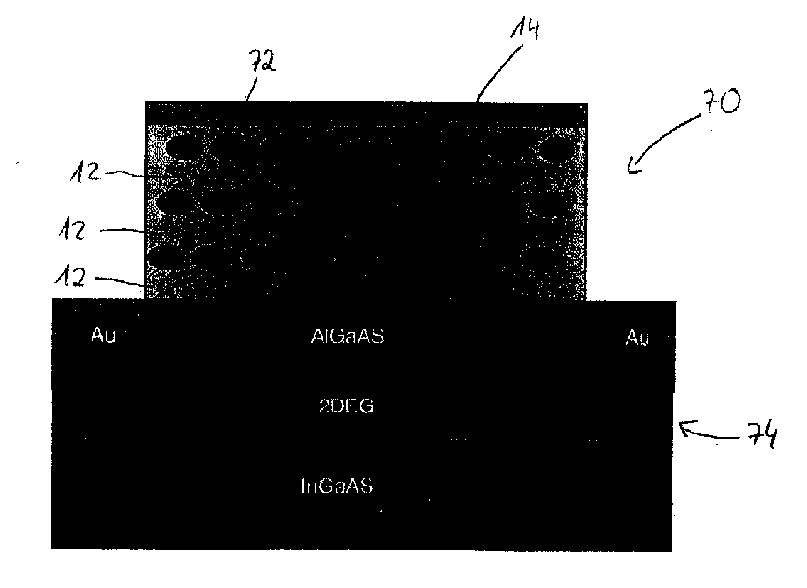
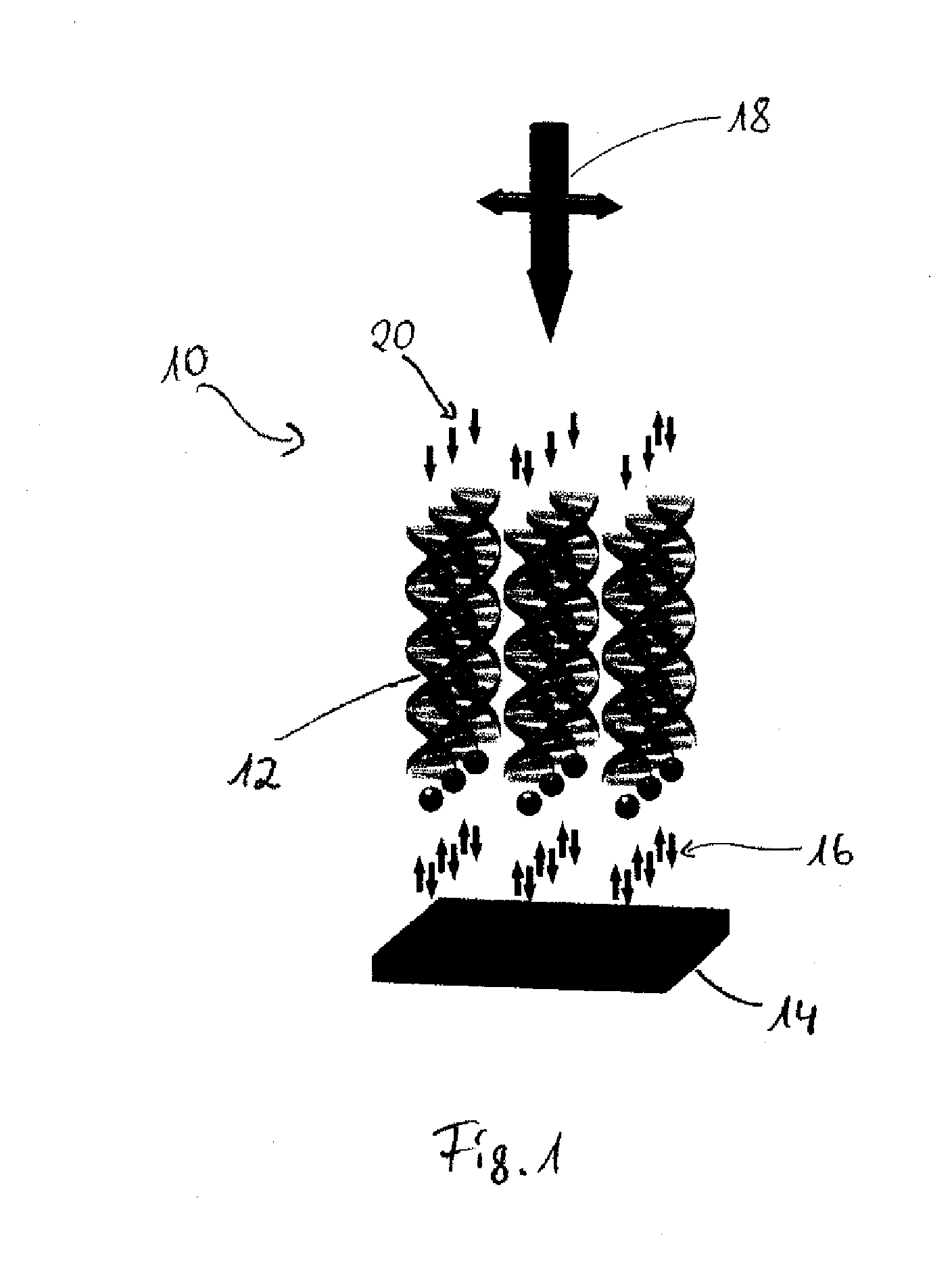
[0062]FIG. 1 shows a perspective view of a spin filter device 10 according to one embodiment of the invention. In this example, the spin filter device 10 includes a mono-layer 12 of double stranded DNA (dsDNA). Thiolated dsDNA is bound to a substrate 14, which is a gold surface in this example, and forms a self-assembled mono-layer 12 of chiral molecules. The substrate can also be formed by any other material, e.g. a different metal or a semiconductor. Unpolarised electrons 16 ejected from the gold surface produced by linearly polarised light 18 incident from the monolayer side are transmitted and can be analyzed. Most of the electrons 20 transmitted through the monolayer 12 are spin polarised. Spin orientation depends on the enantiomer used in the monolayer.

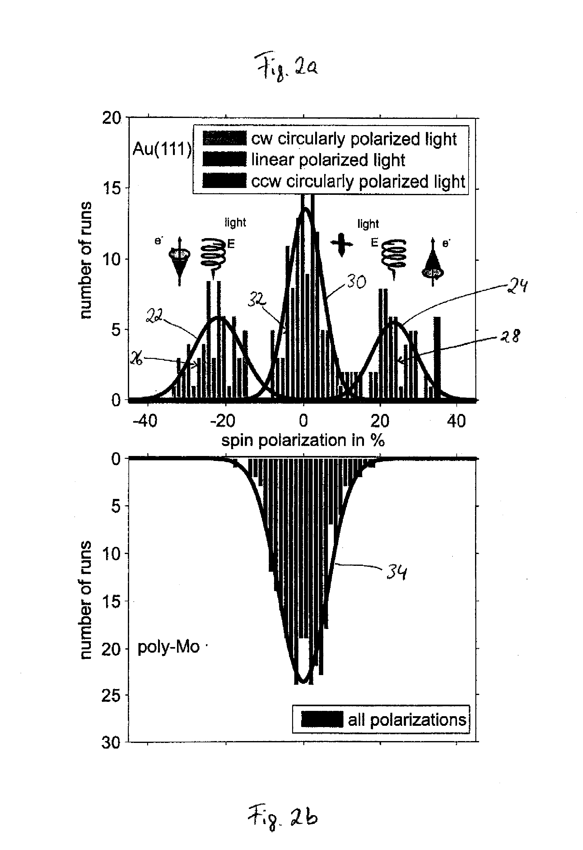
[0063]It is well known that spin-polarised photoelectrons are readily generated from magnetic substrates or when circularly polarised light ejects electrons from substrates with large spin-orbit coupling. Since an organic chiral...


PUM


Abstract

The present invention relates to a method and a device for providing a current of spin-polarised electrons. More particularly, the present invention is suited for use in spin electronics or detection of spin-polarised electrons.

Description

CLAIM OF PRIORITY[0001]This application claims the benefit of priority under 35 U.S.C. §119 (a)-(d) of Great Britain Patent Application Serial Number 1101862.9, entitled “SPIN FILTER DEVICE, METHOD FOR ITS MANUFACTURE AND ITS USE,” filed on Feb. 3, 2011, the benefit of priority of which is claimed hereby, and which is incorporated by reference herein in its entirety.TECHNICAL FIELD[0002]The present invention relates to a method and a device for providing a current of spin-polarised electrons. More particularly, the present invention is suited for use in spin electronics or detection of spin-polarised electrons.BACKGROUND[0003]The generation of a current of spin-polarised electrons, in which all electron spins point mostly in the same direction, is a central aspect of spin electronics (hereafter also called spintronics). Spintronics, or spin electronics, refers to the role played by electron spin in solid state physics, and to devices that specifically exploit spin properties, i.e. s...

Claims


Application Information

Patent Timeline
IPC IPC(8): H01L51/10H01L51/44H01L51/40B82Y25/00
CPCB82Y10/00H01L51/0595H01L51/0093H01L29/66984H10K85/761H10K10/701
Inventor GOHLER, BENJAMINHAMELBECK, VOLKERHANNE, G. FRIEDRICHZACHARIAS, HELMUTNAAMAN, RONMARKUS, TAL ZVI
Owner WESTFALISCHE WILHELMS UNIV MUNSTER
Why Eureka
Try Eureka