Polydimethylsiloxane sheet, optical element incorporating the same, and manufacturing method thereof

Active Publication Date: 2012-09-06
DAI NIPPON PRINTING CO LTD
View PDF6 Cites 10 Cited by
  • Summary
  • Abstract
  • Description
  • Claims
  • Application Information

AI Technical Summary

Benefits of technology

[0029]In such a manufacturing method of the inventive polydimethylsiloxane sheet as described above, the low-content polydimethylsiloxane layer is positioned on the support substrate side, notwithstanding the structure that is the polydimethylsiloxane sheet comprises the high-content polydimethylsiloxane layer having good adhesion to metals,

Problems solved by technology

A problem with the conventional PDMS sheets, however, has been poor adhesion to metals.
Another problem has been that when a PDMS sheet is placed on a silicon-containing substrate such as a glass substrate, a quartz substrate or a silicon substrate to form a metal thin film or a metal pattern of any desired shape thereon, or stored on that substrate over an extended period of time,

Method used


Image

  • Polydimethylsiloxane sheet, optical element incorporating the same, and manufacturing method thereof
  • Polydimethylsiloxane sheet, optical element incorporating the same, and manufacturing method thereof
  • Polydimethylsiloxane sheet, optical element incorporating the same, and manufacturing method thereof

Examples


example 1

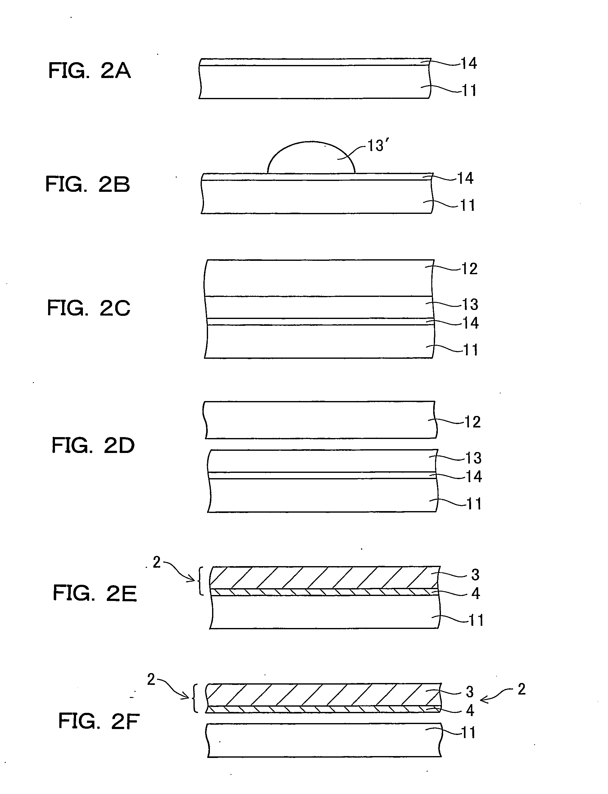
[0104]There was a silicon substrate of 0.625 mm in thickness and 150 mm in diameter provided as the support substrate. This support substrate was found to have a surface average roughness Ra of 0.001 μm as measured on AFM (L-Trace II made by Seiko Instruments Inc.).

[0105]After a polymerization initiator was mixed with a raw material A for the formation of the low-content PDMS layer, the mixture was spin coated on the aforesaid support substrate to form a coating film A. Given the low-molecular-weight siloxane of a cyclic structure represented by [—Si(CH3)2O—]k where k is an integer of 3 to 20 inclusive, that raw material A was a PDMS having a low-molecular-weight siloxane content of 1,000 ppm. The thickness of the coating film A was set such that the low-content PDMS layer formed by curing had a thickness of 0.1 mm.

[0106]Then, after a polymerization initiator was mixed with a raw material B for the formation of the high-content PDMS layer, the mixture (20 grams) was added dropwise t...

example 2

[0108]Example 1 was repeated with the exception that a PDMS having a low-molecular-weight siloxane content of 7,000 ppm was used as the raw material B for the formation of the high-content PDMS layer, thereby preparing a PDMS sheet.

example 3

[0109]Example 1 was repeated with the exception that a PDMS having a low-molecular-weight siloxane content of 200 ppm was used as the raw material A for the formation of the low-content PDMS layer, thereby preparing a PDMS sheet.


PUM

PropertyMeasurementUnit
Fractionaaaaaaaaaa
Fractionaaaaaaaaaa
Thicknessaaaaaaaaaa

Abstract

A PDMS sheet that ensures good adhesion, handleability and stability to metal thin films or metal patterns of any desired shape, an optical element that is kept against de-bonding or exfoliation of metal patterns and has high reliability as well as good handleability and stability, and manufacturing methods thereof. The inventive optical element comprises a polydimethyl-siloxane sheet having a pattern-formation surface defined by one surface and a base surface defined by another surface, and a plurality of metal patterns positioned on the pattern-formation surface. Given a low-molecular-weight siloxane of a cyclic structure represented by [—Si(CH3)2O—]k where k is an integer of 3 to 20 inclusive, polydimethylsiloxane sheet comprises a structure where the content of the low-molecular-weight siloxane at the pattern-formation surface is more than that of the low-molecular-weight siloxane at the base surface, and a spacing between the adjacent metal patterns is variable by deformation of the polydimethylsiloxane sheet.

Description

BACKGROUND OF THE INVENTION[0001]The present invention relates generally to a polydimethylsiloxane sheet, and more particularly to a polydimethylsiloxane sheet for the formation of a metal thin film and a metal pattern shaped as desired, an optical element having a plurality of nano-order metal patterns formed on a flexible resin substrate, and a manufacturing method thereof.[0002]So far, polydimethylsiloxane (hereinafter often abbreviated as PDMS) sheets have been advantageously used in a variety of application fields inclusive of electronic and electric devices or the like because of excelling in heat resistance, cold resistance and weather resistance and having stabilized electric characteristics.[0003]Optical elements having a diffraction grating formed on a glass substrate or the like have also been widely used so far in the art, and more recently, an optical element having a metal pattern formed on a flexible resin substrate has been proposed (the 56th Spring Meeting, 2009—The...

Claims


Application Information

Patent Timeline
IPC IPC(8): G02B5/18B32B3/00B32B7/02B29D11/00B32B27/06
CPCB29D11/00346Y10T428/24355Y10T428/24967B29D11/0074B29D11/00865B29K2083/00B29K2995/0026B29K2995/0034B32B5/145B32B27/283B82Y20/00C09D183/06G02B5/3066H05K1/036Y10T428/31663
Inventor CHIBA, TSUYOSHIFUJITA, HIROSHIARITSUKA, YUKI
Owner DAI NIPPON PRINTING CO LTD
Why Eureka
Try Eureka