Vapor deposition device, vapor deposition method, and semiconductor element manufacturing method

a semiconductor element and vapor deposition technology, applied in the direction of polycrystalline material growth, crystal growth process, chemically reactive gas, etc., can solve the problems of clogging of showerheads, deterioration of material efficiency, and coagulation of partial metallic materials such as cp2mg (biscyclopentadienyl magnesium) in pipes, so as to reduce the loading of carrier gases on the whole, facilitate coagulation, and reduce the effect of gas loading

Inactive Publication Date: 2012-09-06
SHARP KK
View PDF4 Cites 10 Cited by
  • Summary
  • Abstract
  • Description
  • Claims
  • Application Information

AI Technical Summary

Benefits of technology

[0030]According to the present invention, the group V source gas buffer area and the group III source gas buffer area, isolated from each other, filling up the showerhead gas supply mechanism with the respective ones of the aforementioned group V source gas and the group III source gas are stacked so that the group V source gas buffer area is on a gas discharge side.
[0031]Thus, the group III source gas and the group V source gas do not get mixed with each other until the same are introduced into the growth chamber and mixed with each other, and form no products in the showerhead. Therefore, such phenomena are prevented that the source gases react with each other in the showerhead and products adhere to the inner portion when the temperature of the group III source gas buffer area is raised with a temperature raising mechanism so that no metallic material coagulates in the showerhead.
[0032]As to the positional relation between the group III source gas buffer area and the group V source gas buffer area, the group V source gas buffer area is stacked as the gas discharge side for employing a section adjacent to the cooling mechanism for cooling a shower surface as the group V source gas buffer area, thereby preventing such phenomena that the group III source gas buffer area is cooled by the cooling mechanism and a metallic material introduced into the group III source gas buffer area coagulates in the showerhead.
[0033]Also with respect to such a problem that the aforementioned group III source gas introducing pipe and the group V source gas introducing pipe pass through the aforementioned cooling mechanism to introduce the source gases into the growth chamber at the time of gas introduction and hence the metallic material passing through the pipe is cooled by the cooling mechanism to easily coagulate on the wall surface of the pipe, in addition, the group III source gas pipe is prevented from being cooled by the cooling mechanism and coagulation of the metallic material on the pipe wall surface is suppressed by rendering the inner diameter of the group V source gas introducing pipe greater than the outer diameter of the group III source gas introducing pipe and adopting the structure in which the aforementioned group III source gas introducing pipe is inserted into the aforementioned group V source gas introducing pipe in a one-to-one manner.
[0034]According to the above effects, a metallic material, easy to coagulate, such as Cp2Mg (biscyclopentadienyl magnesium), for example, can be properly guided into the growth chamber without coagulating the same in the showerhead in the pipe, and effective film formation can be efficiently performed.
[0035]Further, the source gas introducing pipes are doubled, and the group III source gas containing a large quantity of carrier gas and the group V source gas containing a small quantity of carrier gas are introduced from the inner pipe having a small passage sectional and from the outer side having a large passage sectional area respectively, whereby loadings of the carrier gases on the whole can be reduced, and the cost can be suppressed.

Problems solved by technology

At this time, there is such a problem that a partial metallic material such as Cp2Mg (biscyclopentadienyl magnesium) coagulates in a pipe in the showerhead or on a wall surface in the showerhead due to a temperature drop caused by insufficient temperature control.
Thus, a problem such as deterioration of material efficiency, clogging of the showerhead, deterioration of controllability of a doping concentration or the like is caused.

Method used


Image

  • Vapor deposition device, vapor deposition method, and semiconductor element manufacturing method
  • Vapor deposition device, vapor deposition method, and semiconductor element manufacturing method
  • Vapor deposition device, vapor deposition method, and semiconductor element manufacturing method

Examples


Embodiment Construction

[0051]When describing one embodiment of the present invention on the basis of FIGS. 1 to 11, the same is as follows. In the drawings of this embodiment, it is assumed that the same reference signs denote the same portions or corresponding portions.

[0052]When numbers, quantities and the like are mentioned in the embodiment described below, the range of the present invention is not necessarily restricted to the numbers, the quantities and the like, except a case where description is particularly made. The same reference numerals are assigned to the same components and corresponding components, and there is a case where redundant description is not repeated.

[0053](Basic Structure of Device)

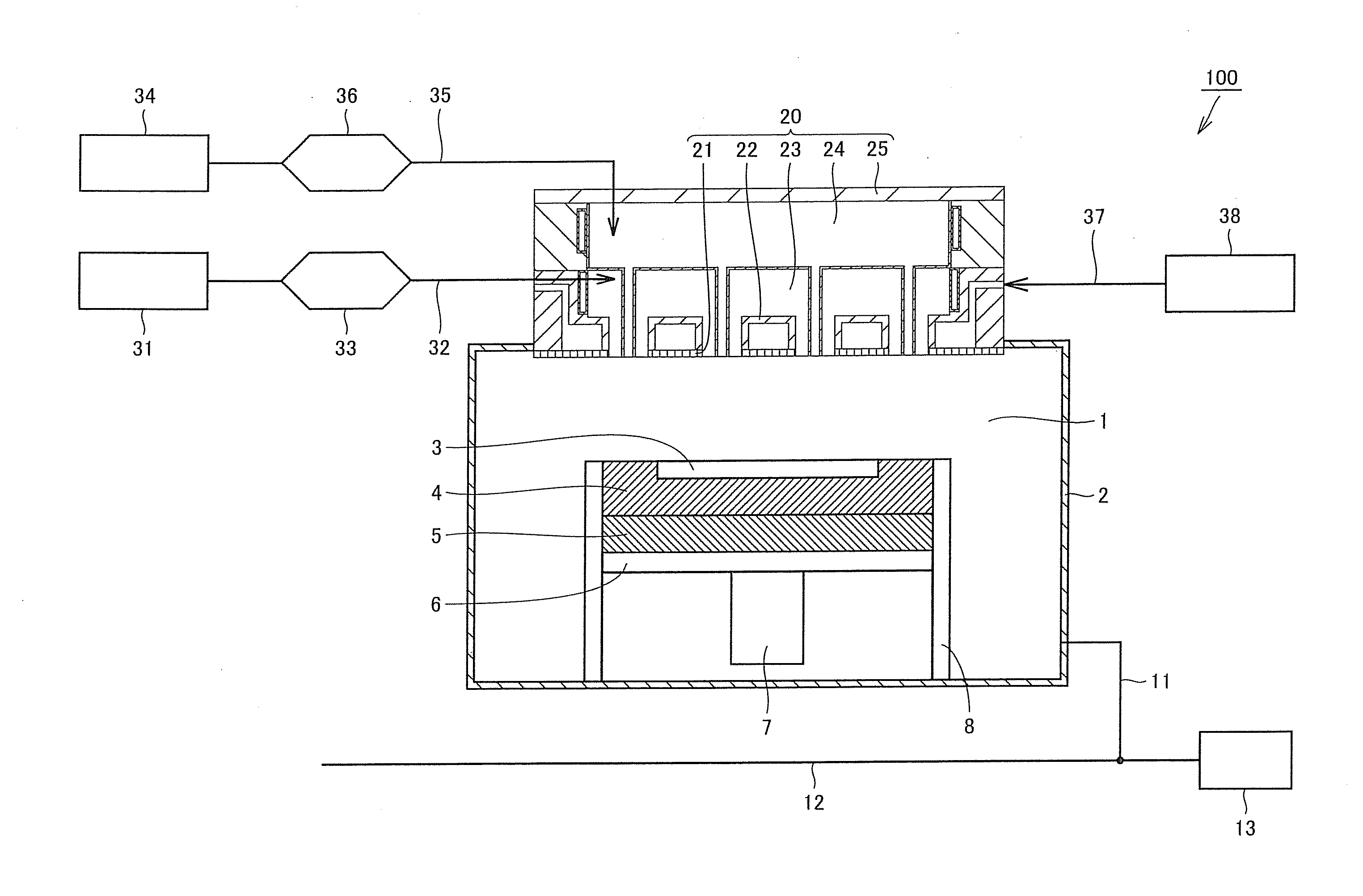
[0054]FIG. 1 shows an example of a schematic structure of a vertical showerhead type MOCVD device 100 which is an example of an MOCVD (Metal Organic Chemical Vapor Deposition) device as a vapor deposition device in an embodiment based on the present invention.

[0055]As shown in FIG. 1, MOCVD device 10...


PUM

PropertyMeasurementUnit
band gapaaaaaaaaaa
inner diameteraaaaaaaaaa
outer diameteraaaaaaaaaa

Abstract

In the disclosed vapor deposition method, by using a structure wherein an inner diameter of a group-V source gas introduction piping is greater than an outer diameter a group-III source gas introduction piping, and the group-III source gas introduction piping is inserted one-to-one into the interior of the group-V source gas introduction piping, the group-III source gas piping is thereby prevented from being cooled by a cooling mechanism, and hardening of metallic materials upon the surface of the wall of the piping is alleviated. It is thus possible to provide a vapor deposition device, a vapor deposition method, and a semiconductor element manufacturing method, which are capable of efficaciously introducing easily hardening metallic materials into a reactor without the metallic materials adhering to a showerhead or a piping, and to carry out efficacious doping.

Description

TECHNICAL FIELD[0001]The present invention relates to a vapor deposition device such as vertical showerhead type MOCVD (Metal Organic Chemical Vapor Deposition) or the like, for example, a vapor deposition method and a semiconductor element manufacturing method.BACKGROUND ART[0002]In general, a thin film of a group III-V semiconductor crystal of GaAs, InGaP or the like is employed in a device such as a light-emitting diode, a semiconductor laser or the like. In recent years, a nitride crystal represented by InGaN or InGaNAs, referred to as a III-V nitride-based semiconductor crystal, has been particularly watched with interest.[0003]InGaN or InGaNAs referred to as the aforementioned III-V nitride-based semiconductor crystal has a band gap of 0.8 eV to 1.0 eV absent in semiconductor crystals other than the aforementioned III-V nitride-based semiconductor crystal such as InGaP or InGaAs, and hence high-efficiency light emission and photoreceiving become possible.[0004]Further, a techn...

Claims


Application Information

Patent Timeline
Patent Type & Authority Applications(United States)
IPC IPC(8): H01L21/205C23C16/30C23C16/455
CPCC23C16/45565C23C16/45572C23C16/45574C30B25/14C23C16/301H01L21/02538H01L21/02579H01L21/0262C30B29/40H01L21/205
Inventor ADACHI, YUSUKESAKAGAMI, HIDEKAZU
Owner SHARP KK
Why Eureka
Try Eureka