
Analog to digital converter circuit

a converter circuit and analog technology, applied in the field of analog to digital converters, can solve the problems of sharp power performance drop and difficult design of high-gain op-amps, and achieve the effect of low power consumption

Active Publication Date: 2012-09-13
UNIVERSITY OF MACAU
View PDF5 Cites 13 Cited by
  • Summary
  • Abstract
  • Description
  • Claims
  • Application Information

AI Technical Summary

Benefits of technology

[0005]Therefore, the object of the present invention is to provide a low power consumption ADC.
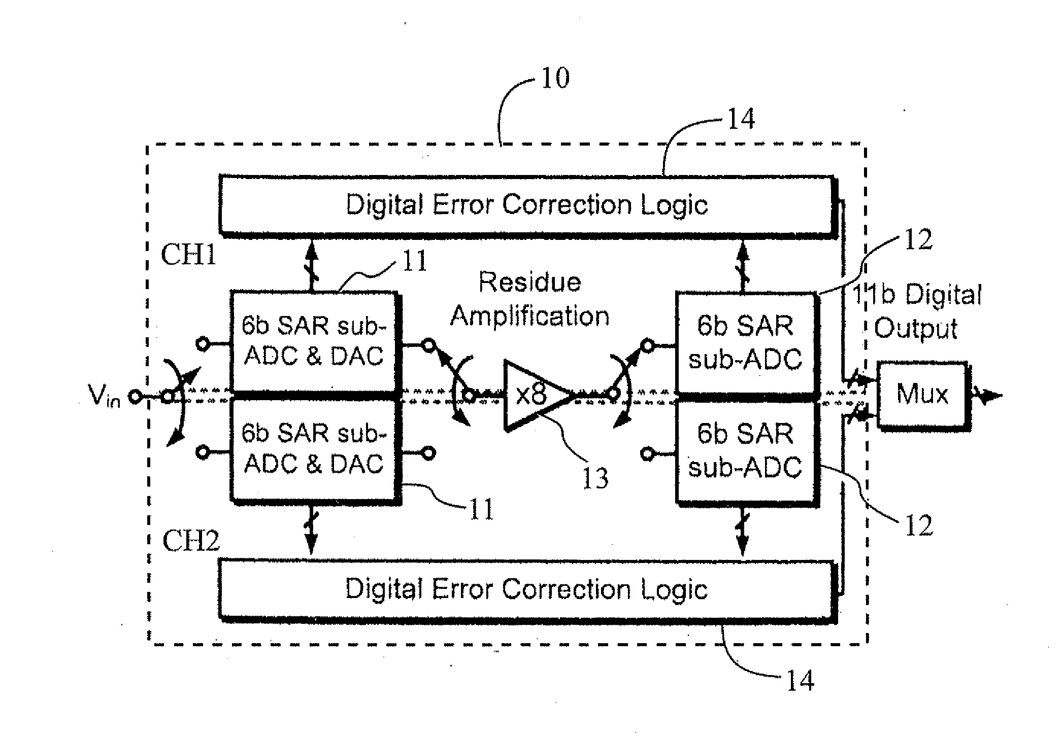
[0007]The gain of the residue amplifier is less than 32 so that the requirements of the gain, the signal amplitude, the noise, the accuracy, the power consumption and the speed of the residue amplifier are relaxed. Preferably, the gain of the residue amplifier is 8.
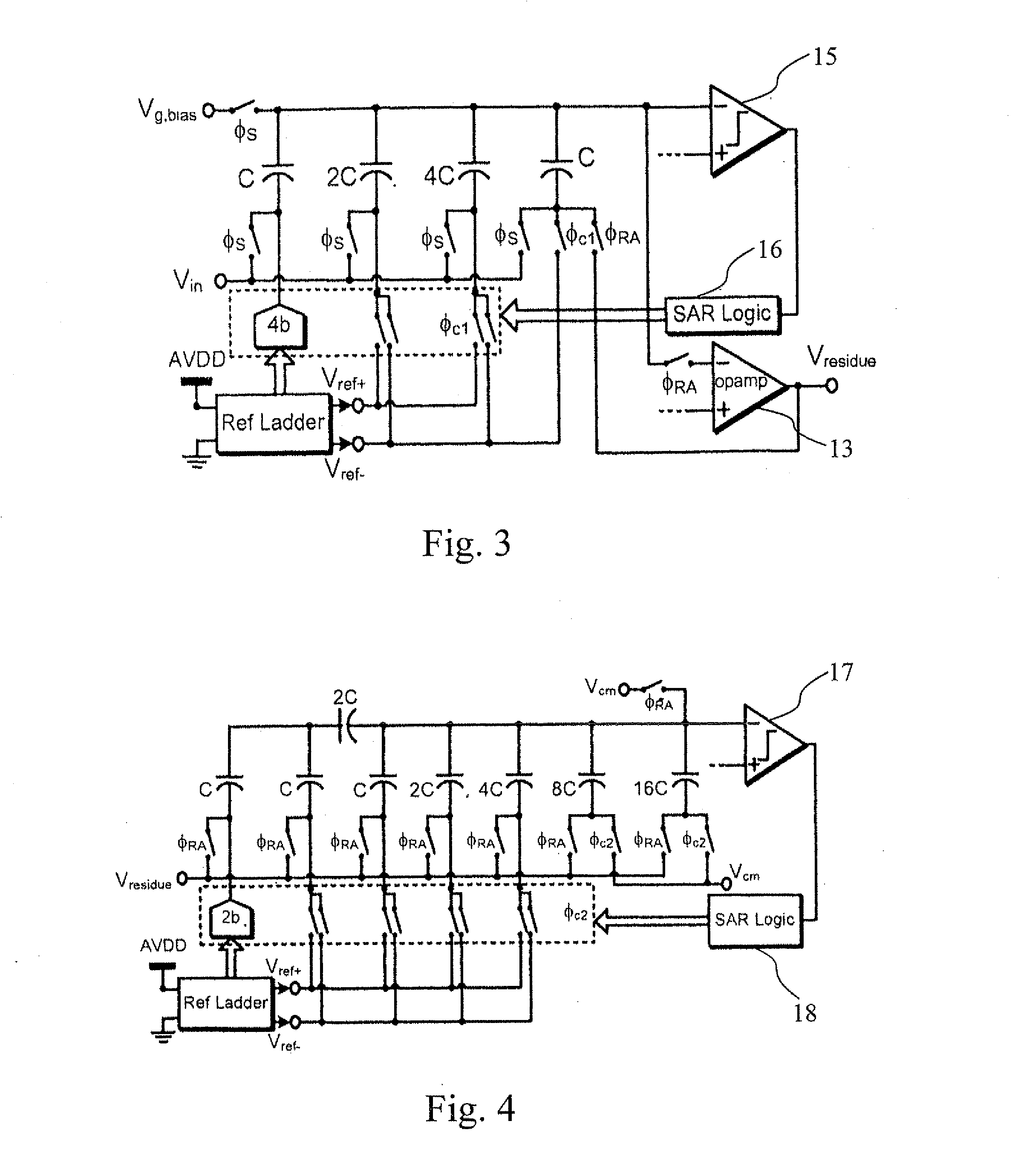
[0008]The first stage SAR sub-ADC comprises a digital to analog converter (DAC) and the digital to analog converter includes a capacitor array that has triple usage to perform input sampling, SAR sub-ADC conversion and residue generation so that input capacitive load, chip area and power consumption can be reduced as a result of elimination of extra capacitor arrays.

Problems solved by technology

The problem becomes more evident with nanometer CMOS technologies because high-gain op-amps are difficult to design.
However, when the resolution goes above 10-bit and the speed is several tens of MHz, the power performance drops sharply.

Method used


Image

  • Analog to digital converter circuit
  • Analog to digital converter circuit
  • Analog to digital converter circuit

Examples


Embodiment Construction

[0015]A preferred embodiment of the present invention will be described hereinafter with reference to the accompanying drawings.

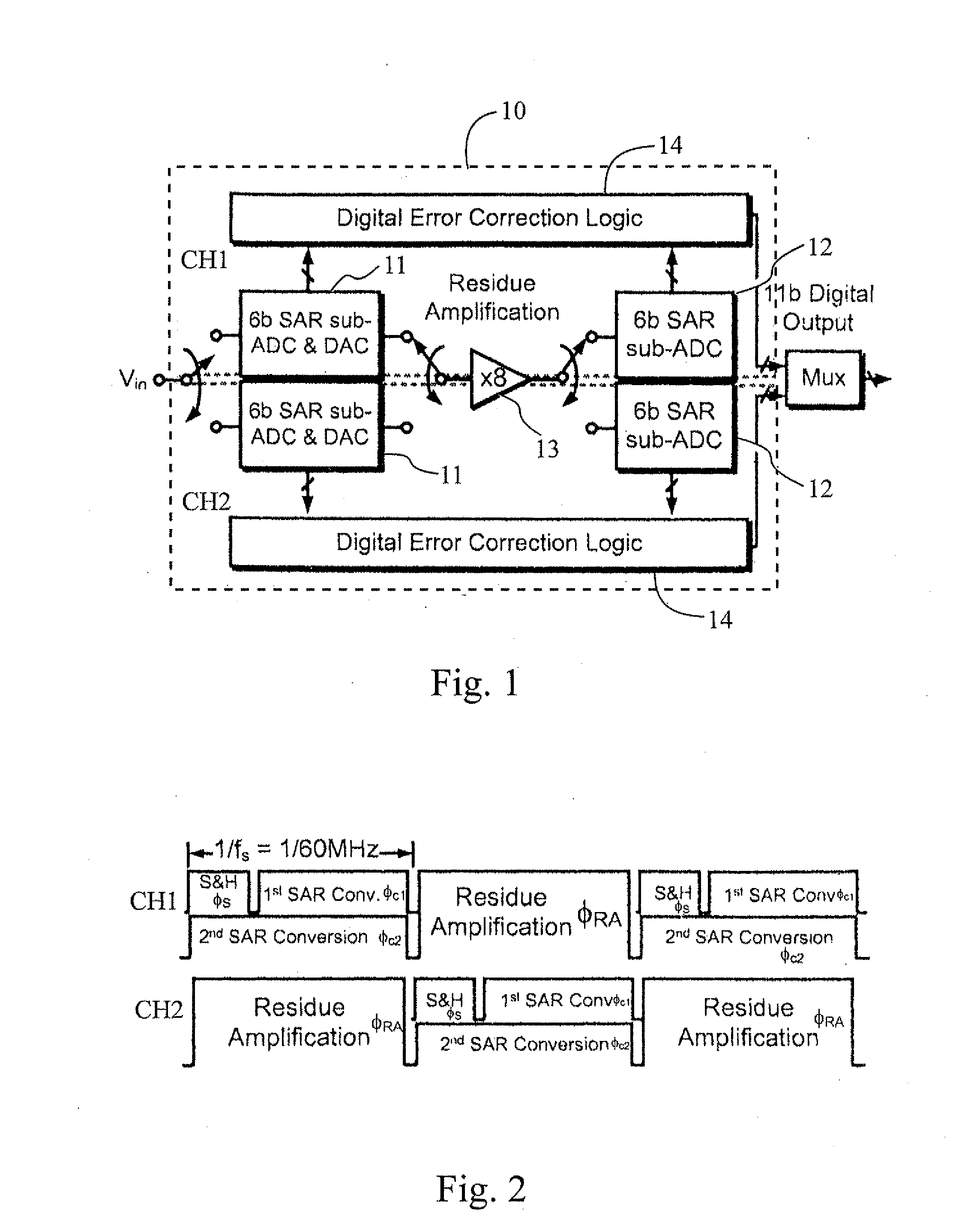
[0016]Reference is now made to FIG. 1. FIG. 1 is a block diagram of an analog to digital converter (ADC) according to an embodiment of the present invention. A two-step time-interleaved successive approximation register (SAR) ADC circuit 10 with 11-bit resolution and 60 MS / s sampling rate is shown in FIG. 1. The ADC circuit 10 includes two time-interleaved two-step SAR ADCs. Each of the SAR ADCs comprises a first stage SAR sub-ADC 11, a second stage SAR sub-ADC 12, a residue amplifier 13 and a digital error correction logic 14.

[0017]The first stage SAR sub-ADC 11, which is a 6-bit ADC, receives an analog input signal Vin and converts the analog input signal Vin to generate a 6-bit digital code. Thus, the first stage SAR sub-ADC 11 converts the coarse 6-bit code. The first stage SAR sub-ADC 11 also generates a residue signal to be amplified by the residue am...


PUM


Abstract

The present invention provides an analog-to-digital converter (ADC) circuit comprising two time-interleaved successive approximation register (SAR) ADCs. Each of the two time-interleaved SAR ADCs comprises a first stage SAR sub-ADC, a residue amplifier, a second stage SAR sub-ADC and a digital error correction logic. The residue amplifier is shared between the time-interleaved paths, has a reduced gain and operates in sub-threshold to achieve power effective design

Description

FIELD OF THE INVENTION[0001]The present invention relates to an analog to digital converter (ADC), and more specifically to two-step time-interleaved successive approximation register (SAR) ADCs.RELATED ART[0002]Typically, an analog-to-digital converter (ADC) is used to convert an input analog voltage (or current) to a digital number proportional to the magnitude of the voltage or current.[0003]A pipelined ADC is a type of ADC including sequence of stages with each stage containing a sub-ADC that generates a residue signal needed to be amplified as an input to the next stage.[0004]The power effectiveness of a traditional two-step or pipelined ADC drops for resolution higher than 10-bit and the sampling rate of 50-100 MS / s because of the power required by the op-amp(s). The problem becomes more evident with nanometer CMOS technologies because high-gain op-amps are difficult to design. With resolution less than 10-bit, a SAR ADC has high power performance with sampling rate around 50 ...

Claims


Application Information

Patent Timeline
Patent Type & Authority Applications(United States)
IPC IPC(8): H03M1/12
CPCH03M1/0695H03M1/1215H03M1/468H03M1/164H03M1/1225
Inventor SIN, SAI-WENGWEI, HE-GONGMALOBERTI, FRANCODING, LIZHU, YANCHAN, CHI-HANGCHIO, U-FATU, SENG-PANMARTINS, RUI PAULO DA SILVA
Owner UNIVERSITY OF MACAU
Learn More