
Semiconductor device based on the cubic silicon carbide single crystal thin film

a single crystal thin film, cubic silicon carbide technology, applied in the direction of semiconductor devices, basic electric elements, electrical equipment, etc., can solve the problems of high quality bulk substrates such as si substrates and gaas substrates that are difficult to manufacture, can not be easily re-crystallized, and can be difficult to manufacture large-scale sic substrates. , the problem of high cos

Active Publication Date: 2012-09-27
OKI ELECTRIC IND CO LTD
View PDF1 Cites 4 Cited by
  • Summary
  • Abstract
  • Description
  • Claims
  • Application Information

AI Technical Summary

Benefits of technology

[0010]Another object of the invention is to provide a low-cost cubic silicon single crystal thin film.

Problems solved by technology

The SiC has a high melting point, and therefore cannot be easily re-crystallized from a melt for growing its bulk crystal.
Thus, high quality bulk substrates such as Si substrates and GaAs substrates are difficult to manufacture.
Also, large size SiC substrates are difficult to manufacture and are therefore extremely expensive as compared to Si substrates and GaSAs substrates.
Thus, the expensive SiC substrate cannot be re-used.

Method used


Image

  • Semiconductor device based on the cubic silicon carbide single crystal thin film
  • Semiconductor device based on the cubic silicon carbide single crystal thin film
  • Semiconductor device based on the cubic silicon carbide single crystal thin film

Examples


first embodiment

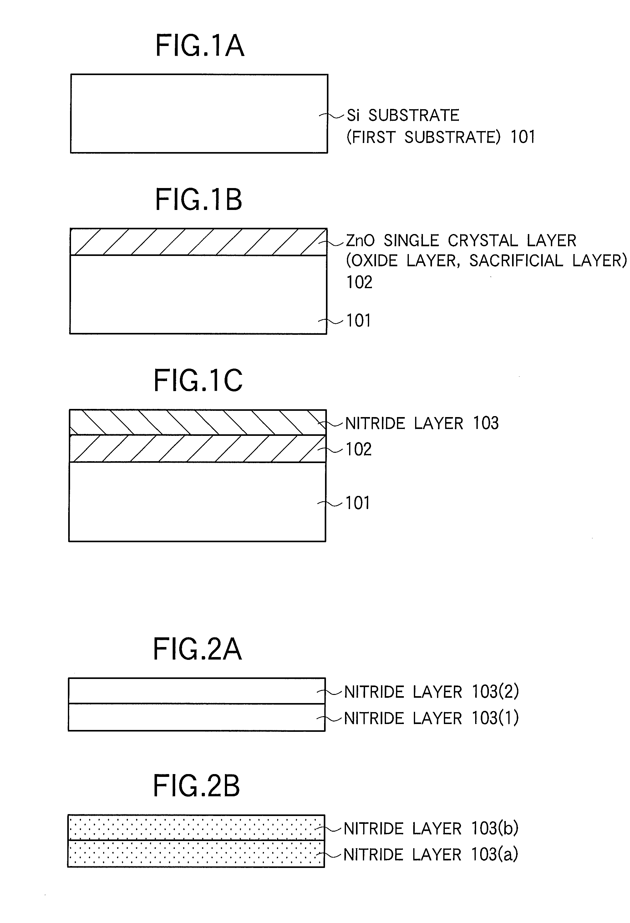
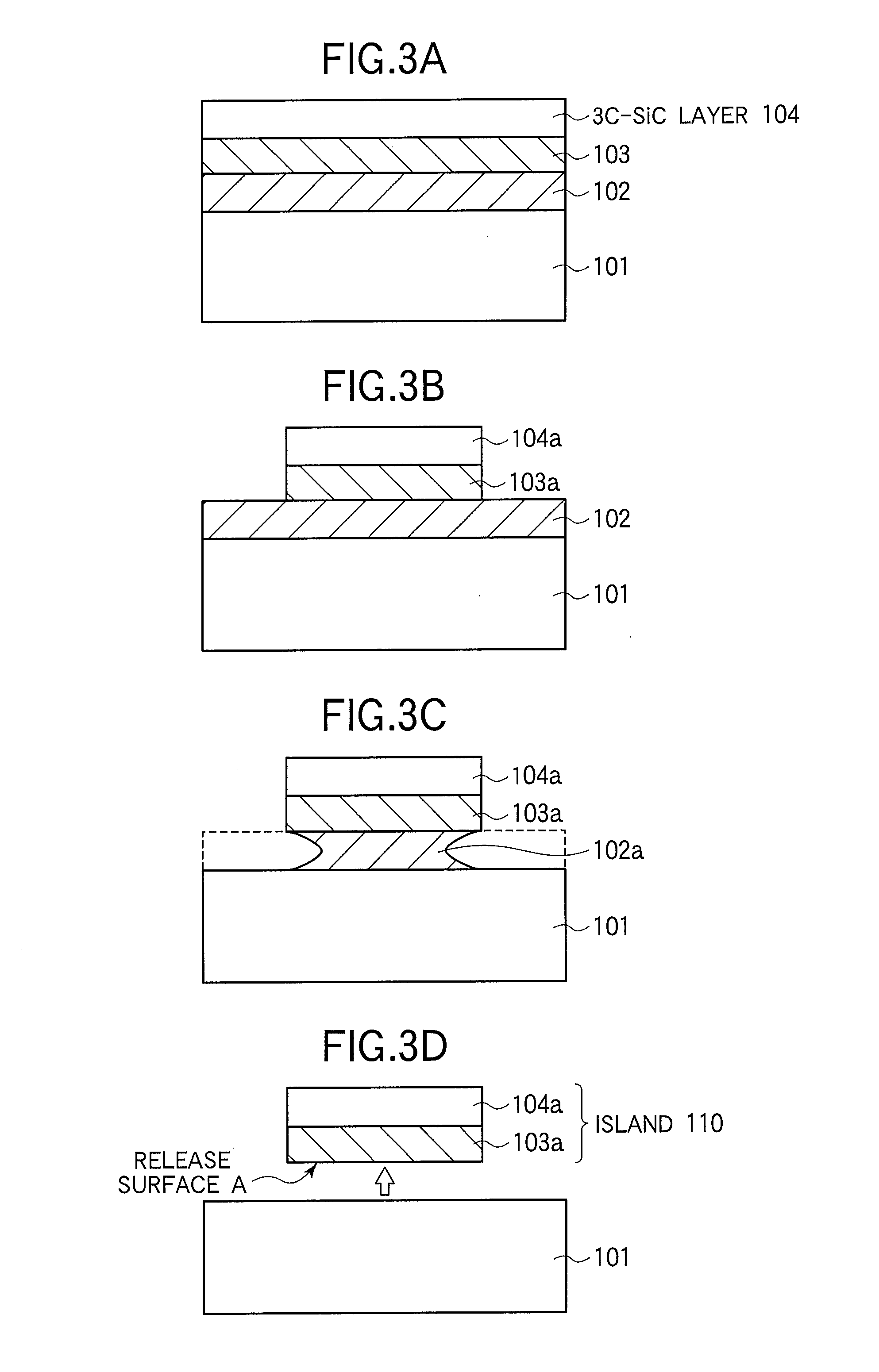
[0029]A first embodiment will be described with reference to FIGS. 1-7. FIGS. 1A-1C illustrate a semiconductor structure including an SiC substrate 101, a ZnO single crystal layer 102, and a nitride layer 103. Referring to FIG. 1A, the SiC substrate 101 is a first substrate, and is preferably an SiC substrate whose crystal structure is hexagonal crystal. In other words, the SiC substrate 101 is either a 4H—SiC substrate or a 6H—SiC substrate. “4H-” indicates a periodic structure of four-atomic layers of hexagonal crystal while “6H-” represents a periodic structure of six-atomic layers of hexagonal crystal.

[0030]Referring to FIG. 1B, an oxide layer, for example, a ZnO single crystal layer 102 is formed as a sacrificial layer on the SiC substrate 101. The ZnO single crystal layer 102 may be formed by molecular beam epitaxy (MBE) or metal organic chemical vapor deposition (MOCVD). A ZnO single crystal is a hexagonal crystal, and therefore a similar hexagonal SiC substrate may be used f...

second embodiment

[0070]A second embodiment differs from the first embodiment in that a first substrate is a sapphire substrate instead of a hexagonal SiC single crystal substrate.

[0071]FIGS. 8A-8D illustrate the configuration of a structure according to the second embodiment in which crystal-grown layers are formed on a substrate. The second embodiment will be described with reference to FIGS. 8A-8D mainly in terms of portions different from the first embodiment.

[0072]FIG. 8A illustrates a first substrate of the second embodiment or a sapphire substrate 211. A sapphire substrate 211 is conveniently used with the surface of the sapphire substrate 211 lying in the (11-21) crystal plane. When the ZnO single crystal layer 102 is formed on the surface of the sapphire substrate 211, the lattice constant of the ZnO single crystal layer 102 substantially matches that of the sapphire substrate 211, preventing defects which would otherwise be caused by substantial mismatching of lattice constants.

[0073]Referr...

modification to second embodiment

[0078]The sapphire substrate 211 employed as the first substrate may be replaced by a nitride semiconductor substrate, for example, an AlxGa1-xN (1≧x≧0) substrate, an InxGa1-xN (1≧x≧0) substrate, or an AlxIn1-xN (1≧x≧0) substrate. For a nitride semiconductor substrate, an AlxGa1-xN (1≧x≧0) (e.g., an AlN layer or a GaN layer) layer may be formed as a buffer layer before a ZnO single crystal layer is formed on the nitride semiconductor substrate. Good lattice matching may be achieved between the nitride semiconductor substrate and the ZnO single crystal layer, allowing formation of a high quality ZnO single crystal layer with less lattice defect.

[0079]The second embodiment allows formation of a high quality 3C—SiC layer on an inexpensive sapphire substrate which serves as the first substrate. Of course, the sapphire substrate as the first substrate can be re-used.


PUM

PropertyMeasurementUnit
temperaturesaaaaaaaaaa
sizeaaaaaaaaaa
depositionaaaaaaaaaa

Abstract

A semiconductor apparatus includes a cubic silicon carbide single crystal thin film of a multilayer structure including an AlxGa1-xAs (0.6>x≧0) layer and a cubic silicon carbide single crystal layer. The apparatus also includes a substrate on which a metal layer is formed. The multilayer structure is bonded to a surface of the metal layer with the AlxGa1-xAs (0.6>x≧0) in direct contact with the metal layer.

Description

[0001]This application is a divisional application of co-pending U.S. application Ser. No. 12 / 662,637, filed Apr. 27, 2010, which claims the benefit of Japan application Serial No. 2009-109281, filed Apr. 28, 2009. These related applications are incorporated herein by reference.BACKGROUND OF THE INVENTION[0002]1. Field of the Invention[0003]The present invention relates to a method for manufacturing a cubic silicon carbide single crystal thin film and a semiconductor device based on the cubic silicon carbide single crystal thin film.[0004]2. Description of the Related Art[0005]Devices formed on a silicon carbide (referred to as SiC hereinafter) substrate are known. One such device is a light emitting diode that includes an n type 6H—SiC epitaxially grown layer and a p type 6H—SiC epitaxially grown layer, both of which being formed on an n type 6H—Si substrate. Japanese Patent Application Laid-Open No. 2000-319099 discloses a device formed on an SiC substrate (e.g., 4H—Si substrate) ...

Claims


Application Information

Patent Timeline
Patent Type & Authority Applications(United States)
IPC IPC(8): H01L29/161
CPCH01L21/0237H01L21/02395H01L21/02463H01L21/02472H01L29/2003H01L21/02529H01L21/7602H01L29/1608H01L21/02502
Inventor OGIHARA, MITSUHIKOSAKUTA, MASAAKI
Owner OKI ELECTRIC IND CO LTD
Learn More