Photodiode and manufacturing method for same, substrate for display panel, and display device

a technology of photodiodes and manufacturing methods, applied in the direction of radioactive devices, instruments, optics, etc., can solve the problems of lowering the heat resistance of the device, reducing the reliability of the device, and reducing the manufacturing yield, so as to achieve high concentration, low impurity concentration, and high concentration

Inactive Publication Date: 2012-09-27
SHARP KK
View PDF10 Cites 33 Cited by
  • Summary
  • Abstract
  • Description
  • Claims
  • Application Information

AI Technical Summary

Benefits of technology

[0061]As described above, the photodiode of the present invention is configured as follows. The first semiconductor layer is a semiconductor layer that has a relatively high concentration of an N-type impurity. The second semiconductor layer is either an intrinsic semiconductor layer or a semiconductor layer that has a relatively low impurity concentration. The third semiconductor layer is a semiconductor layer that has a relatively high concentration of a P-type impurity. One of the first semiconductor layer and the third semiconductor layer is formed on the light receiving surface of the second semiconductor layer so as to overlap the light receiving surface of the second semiconductor layer at least partially in a plan view. The other one of the first semiconductor layer and the third semiconductor layer is formed on an opposite surface of the light receiving surface of the second semiconductor layer so as to overlap the light receiving surface and the one layer at least partially in a plan view. In the second semiconductor layer, the relative light receiving sensitivity to the respective wavelengths of light has the highest value at a wavelength in an infrared region.
[0062]As described above, the display panel substrate of the present invention has a configuration in which the above-mentioned photodiode and an active element are formed on one surface of an insulating substrate.
[0063]As described above, the display device of the present invention is configured to have the above-mentioned display panel substrate and a planar light source device that emits light containing infrared light and visible light in a planar shape.
[0

Problems solved by technology

Further, when a metal is used as the lower electrode 102, the lower electrode 102 is likely to react to the above-mentioned amorphous silicon, thereby causing

Method used


Image

  • Photodiode and manufacturing method for same, substrate for display panel, and display device
  • Photodiode and manufacturing method for same, substrate for display panel, and display device
  • Photodiode and manufacturing method for same, substrate for display panel, and display device

Examples


embodiment 1

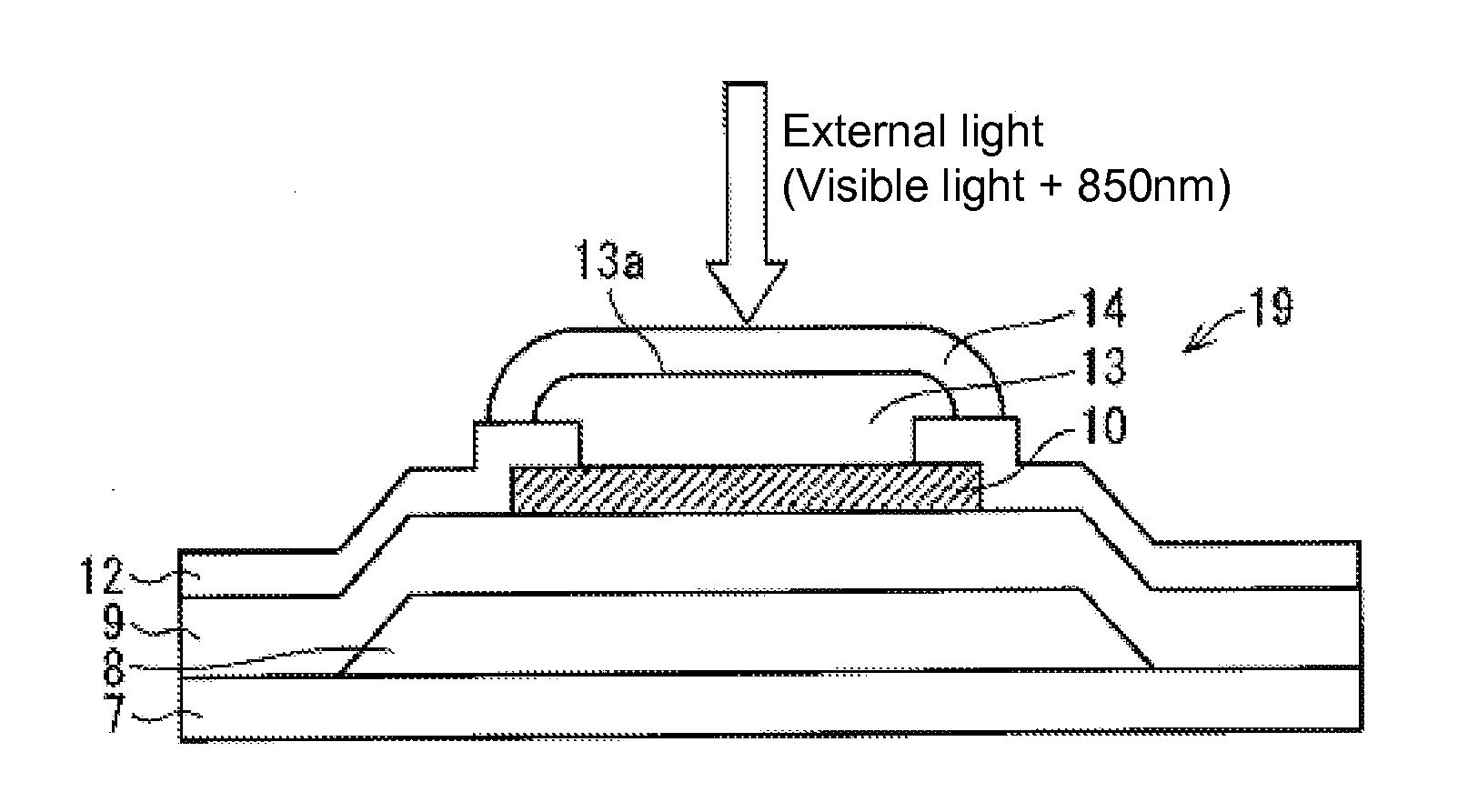
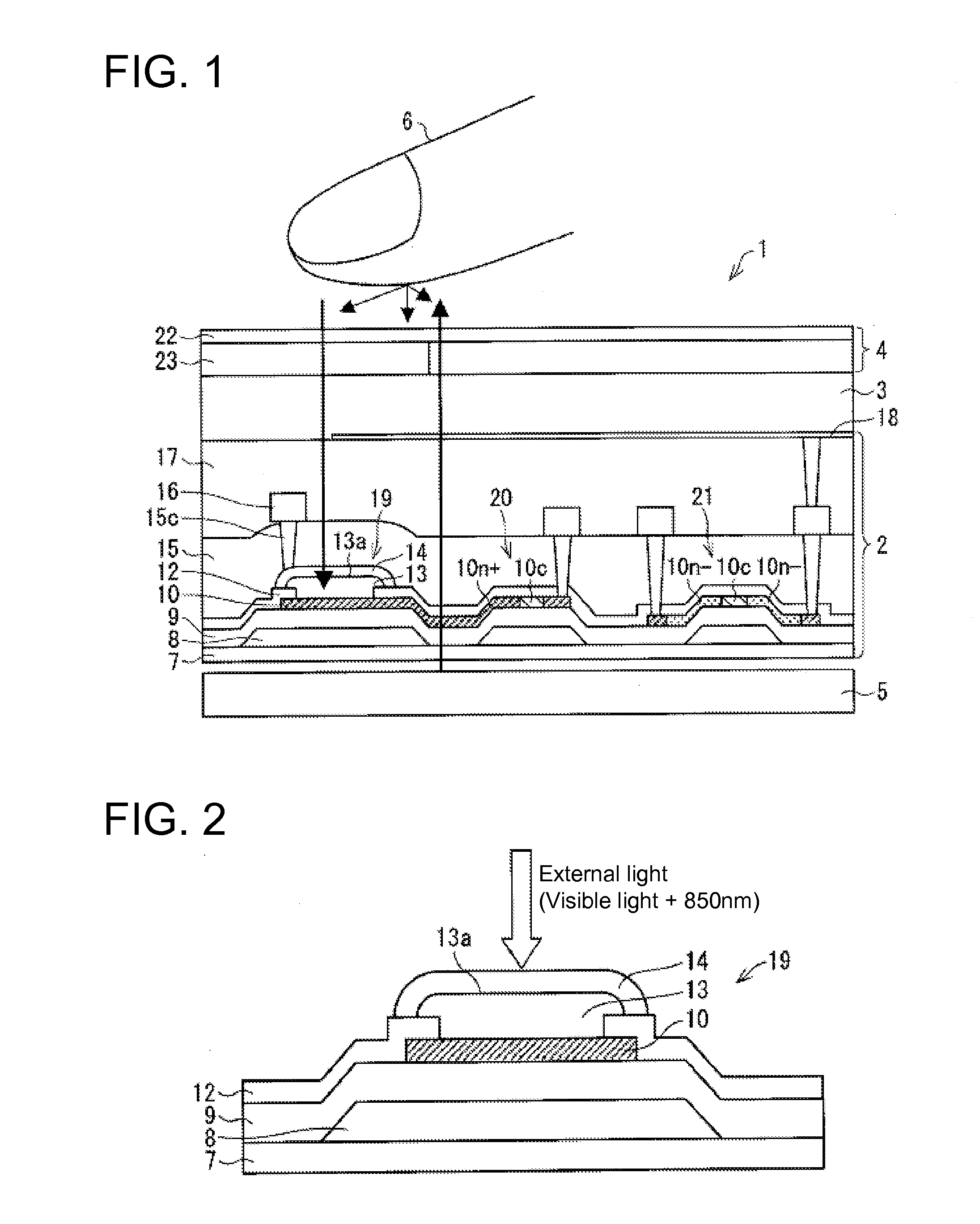
[0092]A configuration of a liquid crystal display device 1, which is an example of a display device according to the present invention, is described below with reference to FIGS. 1 and 2.

[0093]Here, the display device of the present invention is not limited to the liquid crystal display device 1, and can also be realized as an organic EL display device or the like, for example.

[0094]FIG. 1 is a drawing showing a schematic configuration of the liquid crystal display device 1 according to an embodiment of the present invention.

[0095]As shown in FIG. 1, the liquid crystal display device 1 is provided with a liquid crystal display panel that is configured to have an active matrix substrate 2 (display panel substrate) and a color filter substrate 4 disposed so as to face the active matrix substrate 2 and that has a configuration in which a liquid crystal layer 3 is encapsulated between these substrates 2 and 4 by a sealing member.

[0096]Furthermore, the liquid crystal display device 1 has...

embodiment 2

[0191]Next, Embodiment 2 of the present invention is described with reference to FIGS. 13 to 15. The present embodiment is different from Embodiment 1 in that a transparent conductive layer 25 is formed in addition so as to cover the third semiconductor layer 14; that the transparent conductive layer 25 has a portion that does not cover the second semiconductor layer 13 in a plan view; and that the transparent conductive layer 25 is electrically connected to an external wiring line at the non-covering portion. The other configurations are as described in Embodiment 1. In order to facilitate description, members having the same functions as the members shown in drawings of Embodiment 1 are given the same reference characters, and their description is omitted.

[0192]FIG. 13 shows a manufacturing process of a liquid crystal display device 1a according to an embodiment of the present invention.

[0193]After the steps from FIG. 5(a) to FIG. 5(f) and the steps from FIG. 6(a) to FIG. 6(b) wer...

embodiment 3

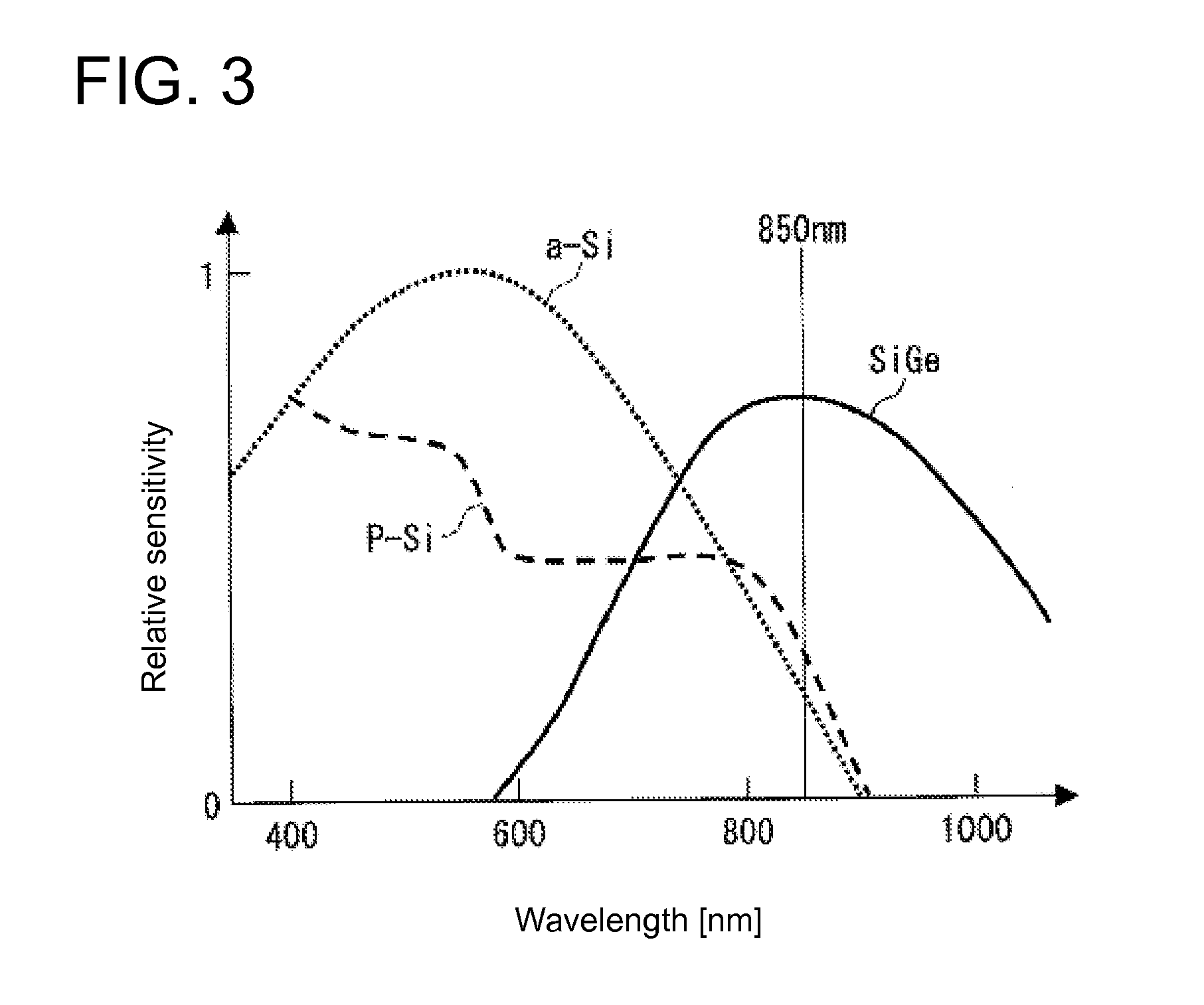
[0212]Next, Embodiment 3 of the present invention is described with reference to FIGS. 17 to 20. The present embodiment is different from Embodiment 1 in that a second photodiode 26 having a light receiving portion that has the highest value at a wavelength in a visible light region and a P-channel TFT element 27 are further provided in addition to the photodiode 19 having the light receiving portion formed of silicon and germanium and the N-channel TFT elements 20 and 21, which are shown in Embodiment 1. Other configurations are as described in Embodiment 1. In order to facilitate description, members having the same functions as the members shown in the figures of Embodiment 1 are given the same reference characters, and their description is omitted.

[0213]A manufacturing process of a liquid crystal display device 1b according to the present embodiment is described below in detail with reference to FIGS. 17 and 18.

[0214]FIGS. 17 and 18 show a manufacturing process of the liquid cry...


PUM


Abstract

A third semiconductor layer 14 is formed on a light receiving surface 13a of a second semiconductor layer 13 so as to cover the light receiving surface 13a of the second semiconductor layer 13 at least partially in a plan view. A first semiconductor layer 10 is formed on an opposite surface of the light receiving surface 13a of the second semiconductor layer 13 so as to overlap the light receiving surface 13a and the third semiconductor layer 14 at least partially in a plan view. In the second semiconductor layer 13, the relative light receiving sensitivity to respective wavelengths of light has the highest value at a wavelength in an infrared region. Thus, even if the intensity of light of the infrared region that is emitted to an object of detection is not increased when sensing by a photodiode is performed using light of the infrared range, it is possible to achieve a photodiode that has a high S/N ratio, which is a ratio of data of received light with respect to noise, and that has high detection accuracy.

Description

TECHNICAL FIELD[0001]The present invention relates to a photodiode (optical sensor), a method of manufacturing the photodiode, a display panel substrate having the photodiode, and a display device having this display panel substrate.BACKGROUND ART[0002]In recent years, a display device in which an optical sensor is provided in a display region of the display device having a plurality of pixels and in a peripheral region that is a region in a periphery of the display region has been developed. Furthermore, the optical sensor can be manufactured in the process of manufacturing pixel TFT elements provided in the display region and driver TFT elements provided in the peripheral region for driving the pixel TFT element.[0003]In addition to a normal display function, this display device can have a touch panel function in which when an input pen, a finger of a person, or the like touches a surface of the display device, for example, the touched position can be detected using a function of ...

Claims


Application Information

Patent Timeline
IPC IPC(8): H01L31/105H01L31/18H01L27/146
CPCH01L27/14632H01L27/14678H01L27/14692G02F2201/58G02F1/13338G02F1/1368G02F2001/136245H01L31/101G02F1/136245
Inventor KATOH, SUMIO
Owner SHARP KK
Why Eureka
Try Eureka