Method for manufacturing semiconductor device, and semiconductor device

a manufacturing method and semiconductor technology, applied in the direction of semiconductor devices, basic electric elements, electrical appliances, etc., can solve the problems of huge device and enormous investment, and difficult to reduce a manufacturing cost, so as to shorten the manufacturing process, reduce the manufacturing cost, and reduce the manufacturing cos

Inactive Publication Date: 2012-09-27
SHARP KK
View PDF11 Cites 206 Cited by
  • Summary
  • Abstract
  • Description
  • Claims
  • Application Information

AI Technical Summary

Benefits of technology

[0040]According to the present invention, a modified region is formed inside a base substrate by multiphoton absorption with the use of a laser having a multiphoton absorption wavelength which laser passes through a silicon surface and is focused inside the silicon substrate. This allows elements such as monocrystalline thin films or elements made of monocrystals to be selectively transferred directly from a non-transparent base substrate onto a large-area transfer destination substrate, although such transfer was difficult according to conventional techniques. Since the elements to be transferred can be directly transferred from the base substrate onto the transfer destination substrate by a single transfer process, highly accurate transfer with little misalignment can be achieved. This shortens a manufacturing process, thereby allowing a reduction in cost.

Problems solved by technology

In addition, since such conventional TFT processes require huge devices such as a vacuum device, a laser crystallization device, and an exposure device, it is difficult to reduce a manufacturing cost.
Accordingly, as the size of mother glass increases (size of tenth generation mother glass: 3.1 m×2.9 m), a huge device and enormous investment are required.
It is therefore difficult to reduce a manufacturing cost.
Moreover, according to this method, only TFTs which largely vary from each other in performance and which require a large amount of power can be obtained.
However, dividing the substrate into millions of elements (each having a size of tens of micrometers) and bonding the elements as in the case of pixel TFTs is impractical not only in terms of throughput but also in terms of handling.
Consequently, the silicon devices cannot be transferred while securing a wide spacing, such as pixel pitch, between the silicon devices.
However, this causes a large decline in use efficiency of the silicon substrate.
Further, according to conventional techniques, it is very difficult to transfer high-performance silicon devices or circuit elements formed on a silicon substrate by a single transfer process so that the silicon devices or the circuit elements are distributed.
Accordingly, it is difficult to selectively transfer only desired monocrystalline silicon devices.

Method used


Image

  • Method for manufacturing semiconductor device, and semiconductor device
  • Method for manufacturing semiconductor device, and semiconductor device
  • Method for manufacturing semiconductor device, and semiconductor device

Examples


first embodiment

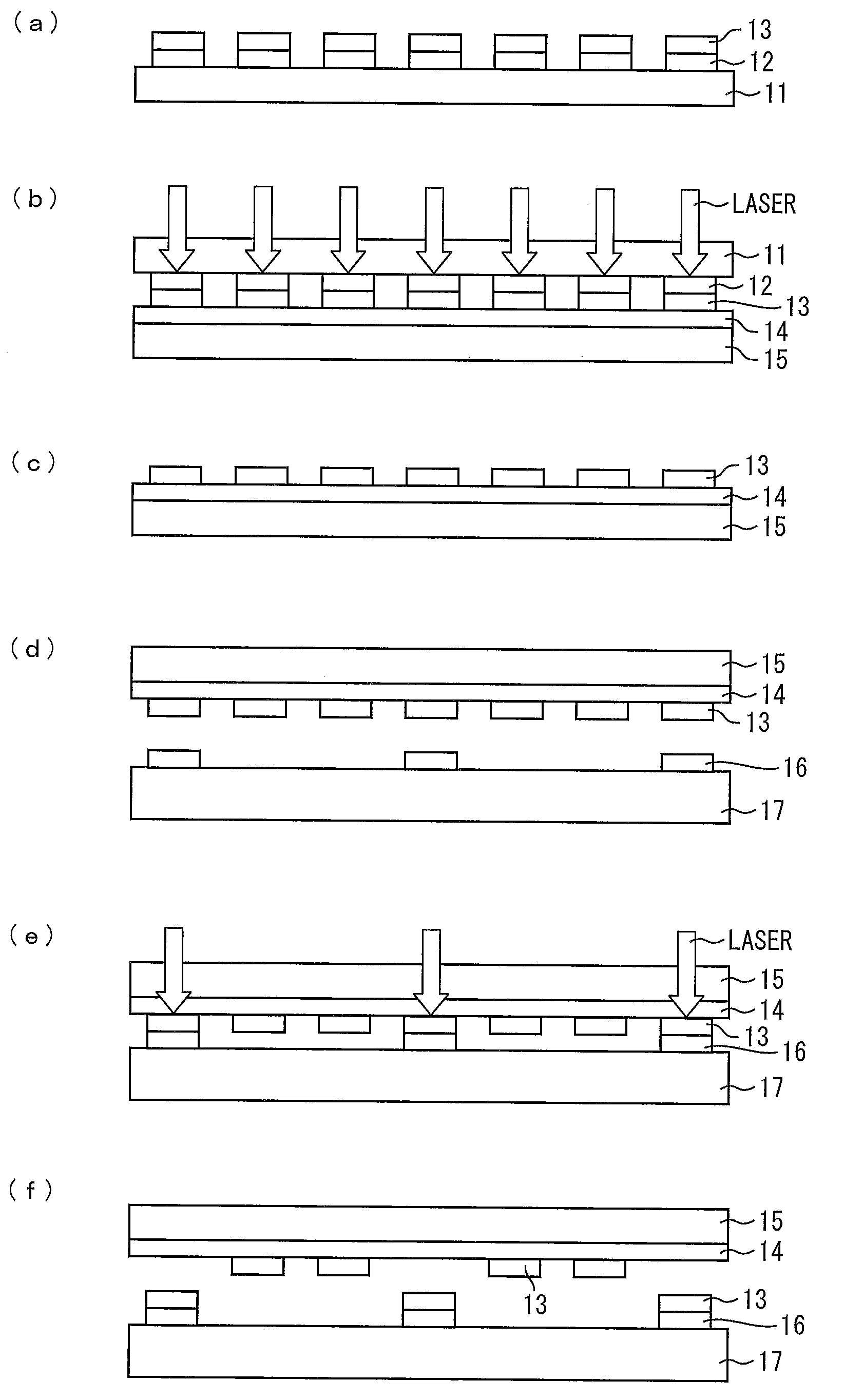
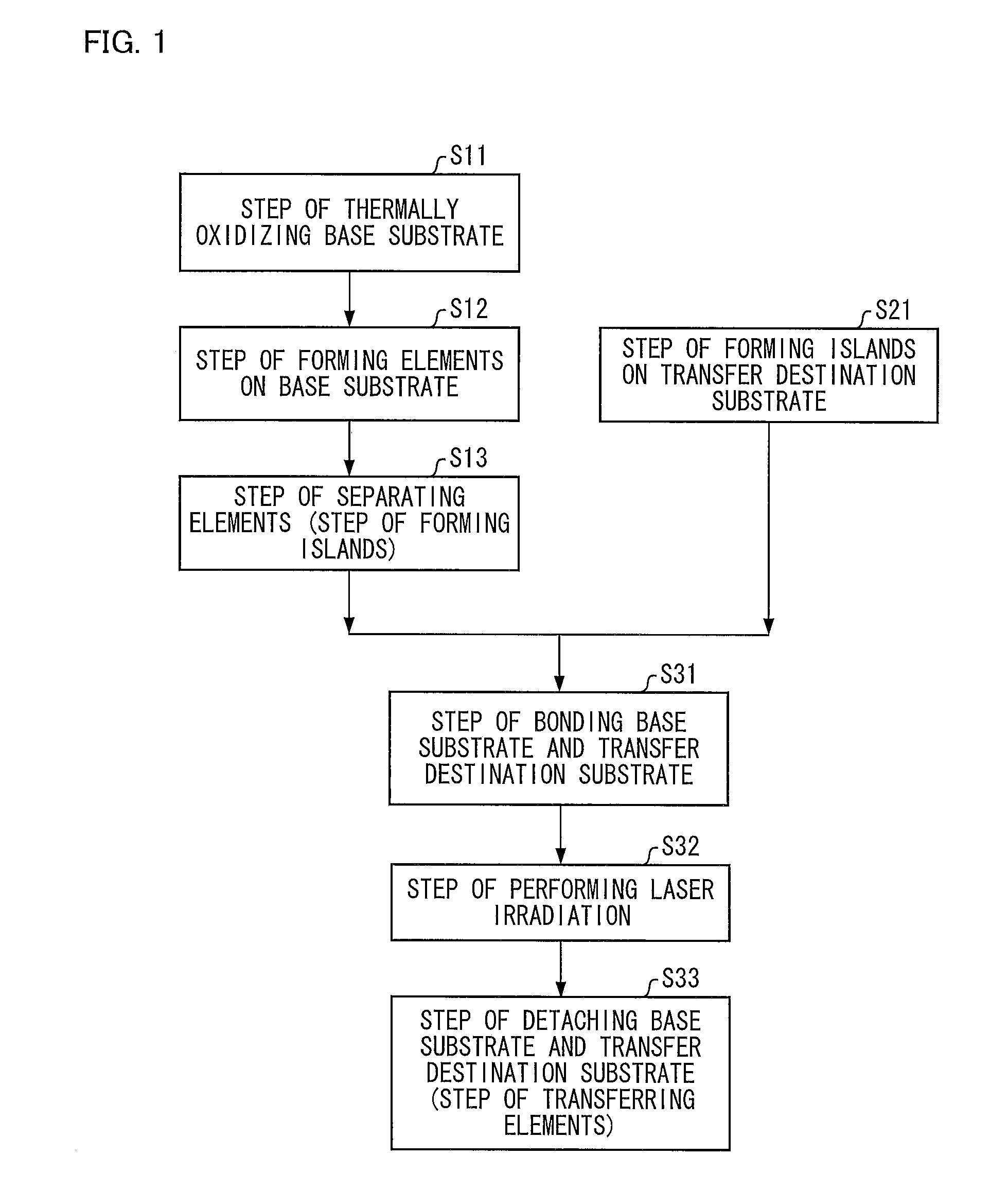
[0078]First Embodiment of the present invention is described below with reference to FIGS. 1 through 4. FIG. 1 is a flow chart showing main steps of the method of the present invention for manufacturing a semiconductor device. FIG. 2 is a cross-sectional view illustrating main steps of a method for forming a base substrate. FIG. 3 is a cross-sectional view illustrating main steps of a method for forming a transfer destination substrate. FIG. 4 is a cross-sectional view illustrating main steps of a method for transferring desired thin films from the base substrate onto the transfer destination substrate.

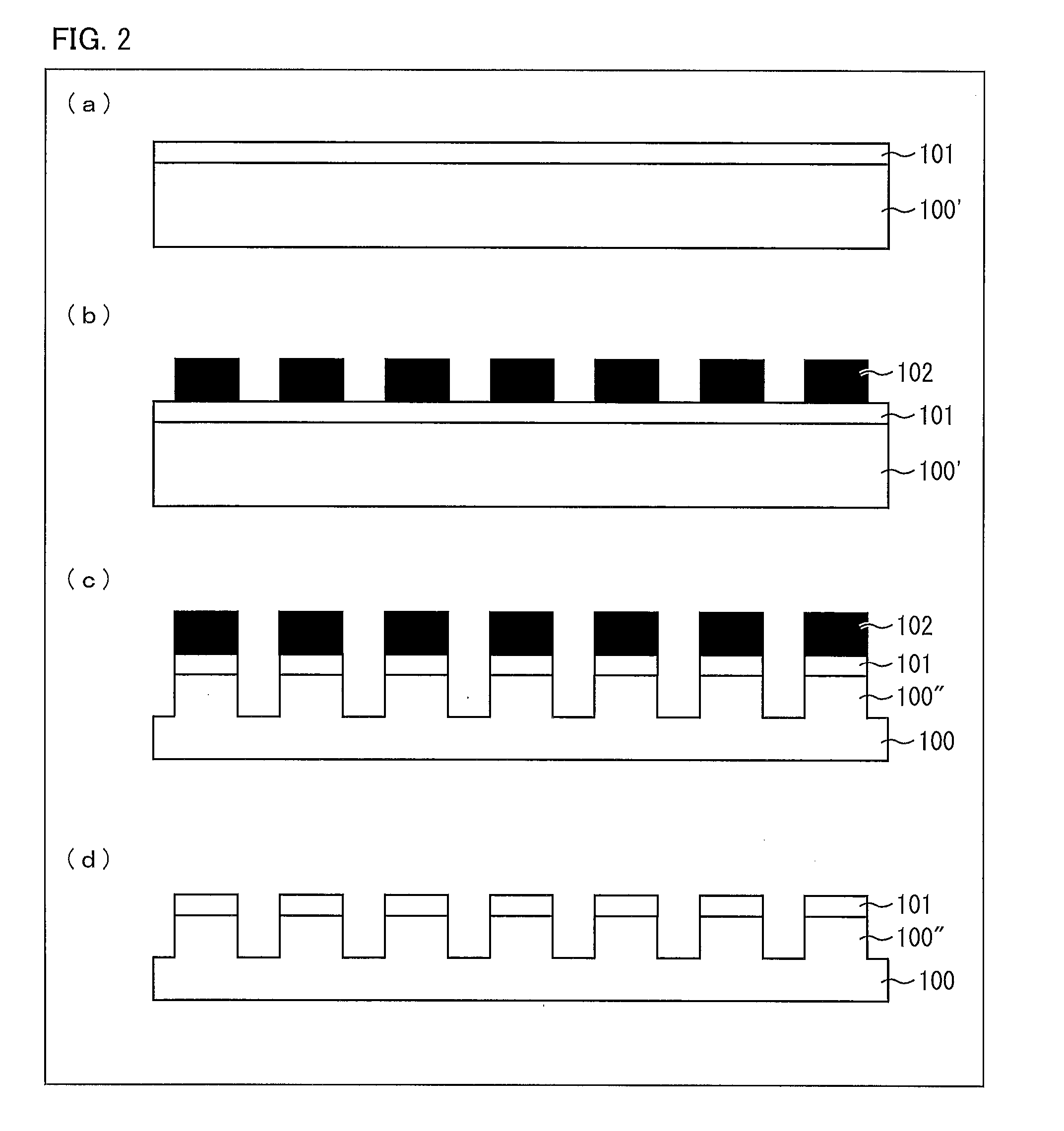
[0079]First, the steps for forming a Si substrate 100 is described with reference to FIG. 2.

[0080]As illustrated in (a) of FIG. 2, a plate-like Si substrate 100′ is thermally oxidized so as to form a thermally-oxidized film 101 having a thickness of approximately 50 nm to 100 nm on a surface of the Si substrate 100′ (S11 of FIG. 1, thermal oxidation step). In the present embodiment, t...

second embodiment

[0101]The present embodiment discusses an example in which monocrystalline Si thin films (elements) formed on a Si substrate are directly transferred onto a glass substrate so that the monocrystalline Si thin films are distributed on the glass substrate, as in First Embodiment. Unlike First Embodiment, the present embodiment discusses an example in which a step of forming, in advance inside the base substrate, a fragile layer that is weaker than other parts of the substrate is added in order to make separation along a modified layer formed in the glass substrate easier.

[0102]FIG. 5 is a cross-sectional view illustrating steps for forming a Si substrate 100 of the present embodiment. Unlike the steps for forming the Si substrate 100 in First Embodiment, the formation process of the Si substrate 100 according to the present embodiment includes a step of forming a fragile layer 104 inside the Si substrate 100 in advance. The steps other than this step are identical to those explained i...

third embodiment

[0108]The present embodiment discusses an example in which, instead of the fragile layer, a light absorbing layer which absorbs more light than the other parts of the substrate is formed in advance inside the main body of the base substrate in order to make the separation along the modified layer formed inside the Si substrate easier. Steps other than the light absorbing layer formation step are identical to those described in First and Second Embodiments, and are therefore described briefly. Note that the present embodiment is described with reference to identical drawings to those of Second Embodiment.

[0109]In the formation process of the Si substrate 100 according to the present embodiment, first, a thermally-oxidized film 101 is formed on a plate-like Si substrate 100′ as illustrated in (a) of FIG. 5, and then a light absorbing layer 105 is formed inside the Si substrate 100′ as illustrated in (b) of FIG. 5.

[0110]Specifically, an ion is implanted into the Si substrate 100′ at a ...


PUM


Abstract

The present invention provides a method for selectively transferring elements such as monocrystalline Si thin films or elements made of monocrystalline Si from a base substrate (100) onto an insulating substrate without the use of an intermediate substrate. The base substrate (first substrate) (100) in which the elements are formed is selectively irradiated with a laser having a multiphoton absorption wavelength. Thus, elements to be transferred out of the elements and corresponding thin films on the base substrate (100) are transferred onto a transfer destination substrate (second substrate) (200).

Description

TECHNICAL FIELD [0001]The present invention relates to a method for manufacturing a semiconductor device, especially to a method for transferring monocrystalline thin films or semiconductor elements made of monocrystal onto an insulating substrate so that the monocrystalline thin films or the semiconductor elements are distributed on the insulating substrate.BACKGROUND ART [0002]Currently, production of a super-high-performance low-cost display requires both of (i) TFT (Thin Film Transistor) performance equivalent to that attained with the use of monocrystalline silicon and (ii) a reduction in manufacturing cost. According to conventional TFT processes such as a process using amorphous silicon (hereinafter referred to as “a-Si”) and a process using polycrystalline silicon (hereinafter referred to as “poly-Si”), a TFT having desired performance cannot be obtained. In addition, since such conventional TFT processes require huge devices such as a vacuum device, a laser crystallization ...

Claims


Application Information

Patent Timeline
Patent Type & Authority Applications(United States)
IPC IPC(8): H01L29/06H01L21/265
CPCH01L21/76254H01L27/1214H01L27/1266H01L21/6835H01L27/12H01L2221/68368H01L2221/68381H01L21/26H01L2221/68322H01L2221/68363
Inventor MITANI, MASAHIRO
Owner SHARP KK
Why Eureka
Try Eureka