Method for manufacturing semiconductor device

Active Publication Date: 2012-10-04
SEMICON ENERGY LAB CO LTD
View PDF5 Cites 13 Cited by
  • Summary
  • Abstract
  • Description
  • Claims
  • Application Information

AI Technical Summary

Benefits of technology

[0018]According to one embodiment of the present invention, the amount of water and hydrogen contained in an oxide semiconductor film can be reduced, and oxyge

Problems solved by technology

However, such a semiconductor device has a problem in reliability.
On the other hand, in a semiconductor device in which an oxide semiconductor film is used for a channel formation region, when many oxygen deficiencies are contained in the oxide semiconductor film, t

Method used


Image

  • Method for manufacturing semiconductor device
  • Method for manufacturing semiconductor device
  • Method for manufacturing semiconductor device

Examples


embodiment 1

[0034]In this embodiment, a method for manufacturing a semiconductor device according to one embodiment of the present invention will be described.

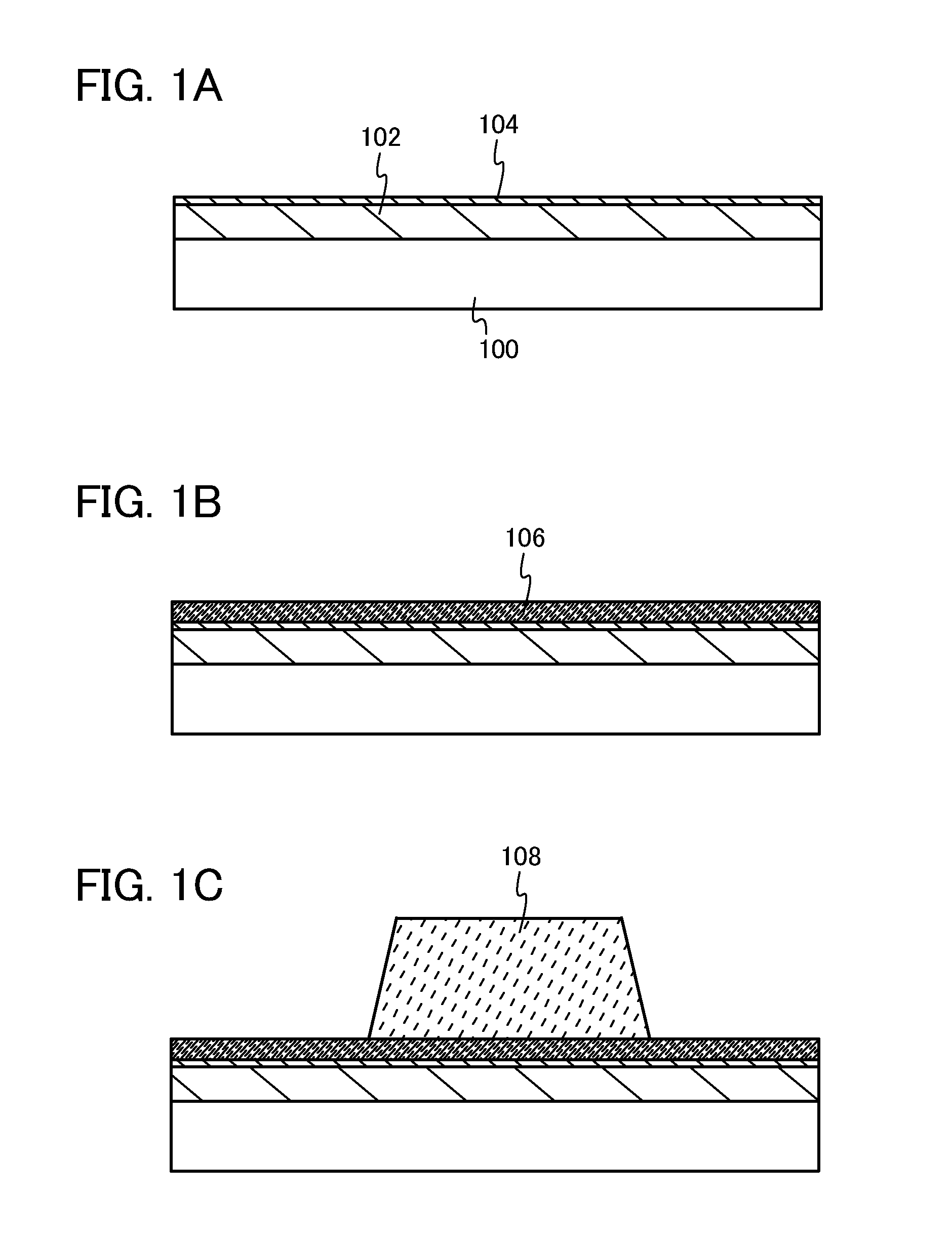
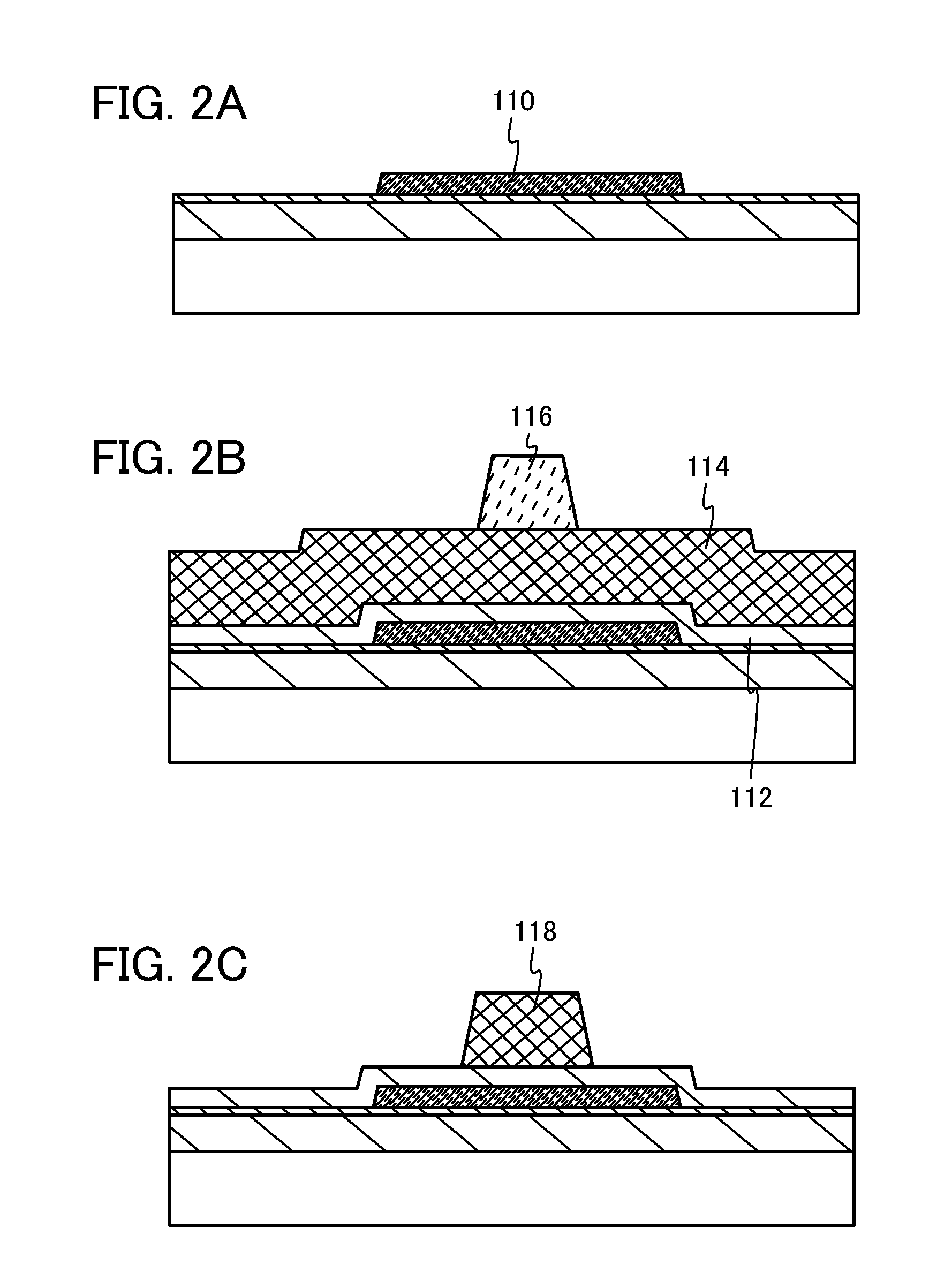
[0035]First, a stacked base film including a first base film 102 and a second base film 104 is formed over a substrate 100 (see FIG. 1A). Next, a first heat treatment is performed after the second base film 104 is formed. The first heat treatment is a step in which water and hydrogen are desorbed from the stacked base film while desorption of oxygen from the stacked base film is suppressed.

[0036]As the substrate 100, a glass substrate (preferably a non-alkali glass substrate), a quartz substrate, a ceramic substrate, a plastic substrate, or the like can be used as appropriate. Alternatively, a flexible glass substrate or a flexible plastic substrate can be used as the substrate 100. For a plastic substrate, a material having low refractive index anisotropy is preferably used. For example, polyether sulfone (PES), a polyimide film, polyeth...

embodiment 2

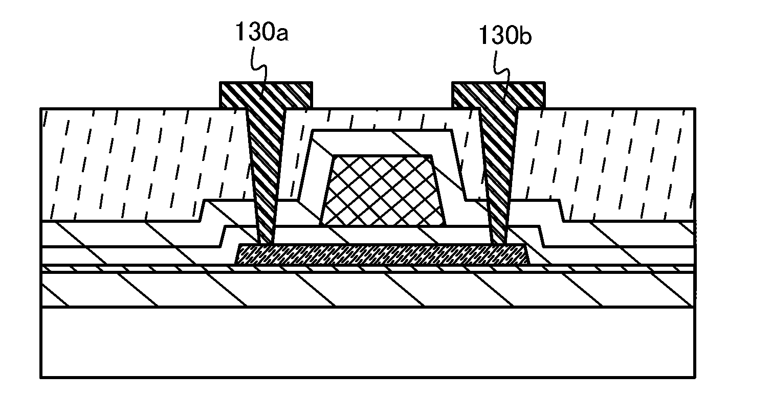
[0150]The semiconductor device (transistor) described in Embodiment 1 can be used as a pixel transistor of a display device.

[0151]In a pixel transistor in this embodiment, an island-shaped transparent conductive film serving as a pixel electrode may be formed selectively so as to be connected to at least one of the source electrode 130a and the drain electrode 130b in the transistor which is formed by the manufacturing method described in Embodiment 1.

[0152]However, there is no limitation thereto, and the island-shaped transparent conductive film may be formed selectively by an ink-jet method so as to be connected to one of the source electrode 130a and the drain electrode 130b.

[0153]The transparent conductive film can be formed using a conductive composition containing a conductive high molecule (also referred to as a conductive polymer) having a light-transmitting property. It is preferable that the transparent conductive film formed using the conductive composition have a sheet ...

embodiment 3

[0156]A semiconductor device according to one embodiment of the present invention, to which the semiconductor device of in Embodiment 1 or 2 is applied, includes electronic paper. Electronic paper can be used for electronic appliances of a variety of fields as long as they can display data. For example, electronic paper can be applied to an electronic book reader (e-book), a poster, a digital signage, a public information display (PID), an advertisement in a vehicle such as a train, displays of various cards such as a credit card, and the like. An example of such electronic appliances is illustrated in FIG. 4.

[0157]FIG. 4 illustrates an example of an electronic book reader. For example, an electronic book reader 300 includes two housings 301 and 303. The housings 301 and 303 are combined with each other with a hinge 311 so that the electronic book reader 300 can be opened and closed with the hinge 311 as an axis. With such a structure, the electronic book reader 300 can be handled l...


PUM


Abstract

The amount of water and hydrogen contained in an oxide semiconductor film is reduced, and oxygen is supplied sufficiently from a base film to the oxide semiconductor film in order to reduce oxygen deficiencies. A stacked base film is formed, a first heat treatment is performed, an oxide semiconductor film is formed over and in contact with the stacked base film, and a second heat treatment is performed. In the stacked base film, a first base film and a second base film are stacked in this order. The first base film is an insulating oxide film from which oxygen is released by heating. The second base film is an insulating metal oxide film. An oxygen diffusion coefficient of the second base film is smaller than that of the first base film.

Description

BACKGROUND OF THE INVENTION[0001]1. Field of the Invention[0002]The present invention relates to a method for manufacturing a semiconductor device. Note that in this specification, a semiconductor device refers to a semiconductor element itself or a device including a semiconductor element. As an example of such a semiconductor element, for example, a transistor (a thin film transistor and the like) can be given. In addition, a semiconductor device also refers to a display device such as a liquid crystal display device.[0003]2. Description of the Related Art[0004]In recent years, a semiconductor device in which an oxide semiconductor film is used for a channel formation region has attracted great attention (see Patent Documents 1 and 2, for example).REFERENCEPatent Document[0005][Patent Document 1] Japanese Published Patent Application No. 2007-123861[0006][Patent Document 2] Japanese Published Patent Application No. 2007-096055SUMMARY OF THE INVENTION[0007]A semiconductor device in...

Claims


Application Information

Patent Timeline
IPC IPC(8): H01L21/36H01L21/283
CPCH01L21/02565H01L21/0242H01L21/02502H01L21/02658H01L21/02422H01L29/517H01L21/02554H01L29/7869H01L29/513H01L21/02488H01L29/66742H01L29/78603H01L29/66969
Inventor IMOTO, YUKISATO, YUHEI
Owner SEMICON ENERGY LAB CO LTD
Why Eureka
Try Eureka