

Dicing die-bonding film
- Summary
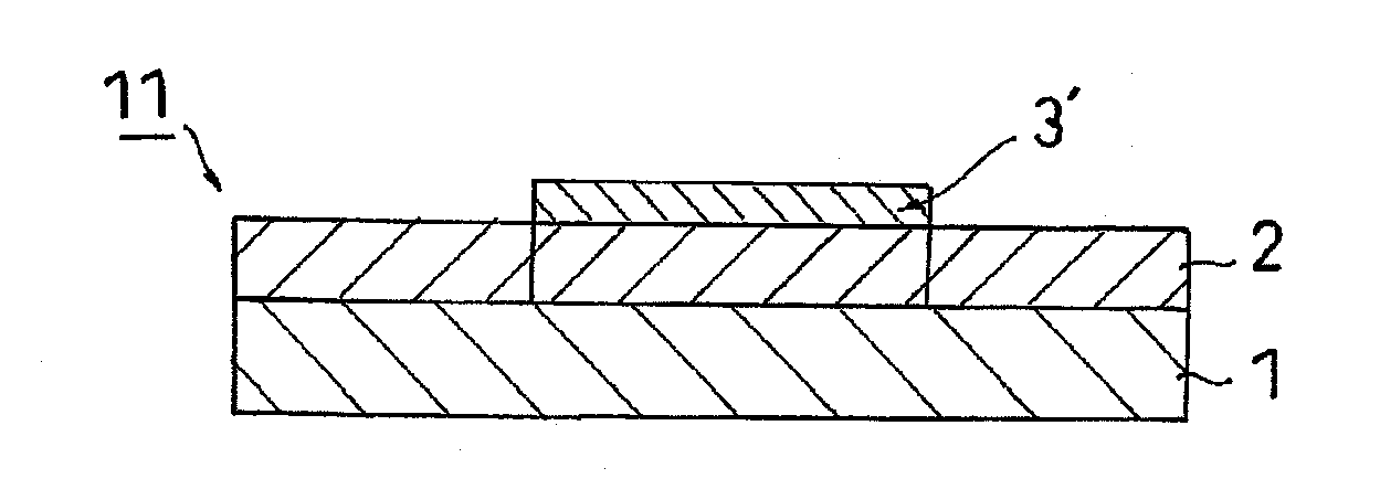
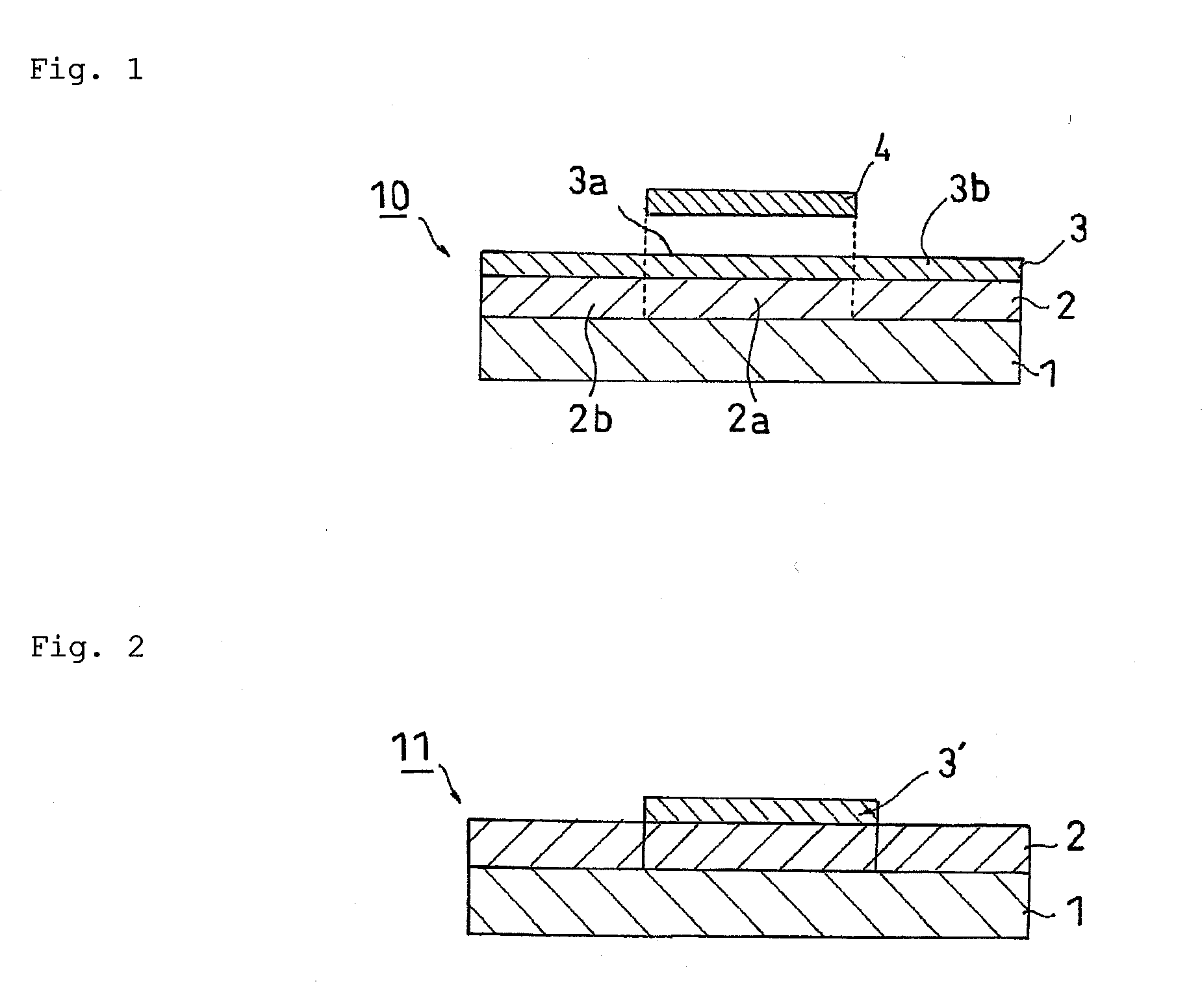
- Abstract
- Description
- Claims
- Application Information
AI Technical Summary
Benefits of technology
Problems solved by technology
Method used
Image

Examples
example 1
[Production of Die-Bonding Film]
[0117]3 parts by weight of a multifunctional isocyanate crosslinking agent, 23 parts by weight of an epoxy resin (Epicoat 1004, manufactured by Japan Epoxy Resins Co., Ltd.), and 6 parts by weight of a phenol resin (Milex XLC-CC, manufactured by Mitsui Chemicals, Inc.) were dissolved in methylethylketone with respect to 100 parts of an acrylic ester polymer (Paracron W-197CM, manufactured by Negami chemical Industries Co., Ltd.) having ethyl acrylate-methyl methacrylate as a main component, to prepare a solution of an adhesive composition having a concentration of 20% by weight.
[0118]The solution of an adhesive composition was applied onto a release-treated film composed of a polyethylene terephthalate film as a release liner (thickness 50 μm) on which a silicone release treatment was performed. Then, it was dried at 120° C. for 3 minutes to produce a die-bonding film A having a thickness of 25 μm on the release-treated film.
[Production of Dicing Film...
example 2
[Production of Die-Bonding Film]
[0124]In Example 2, a die-bonding film B (thickness 50 μm) according to Example 2 was produced in the same manner as in Example 1 except that a polymer (Paracron SN-710, manufactured by Negami chemical Industries Co., Ltd.) having butyl acrylate as a main component was used instead of the acrylic ester polymer used in Example 1.
[Production of Dicing Film]
[0125]First, a radiation curing-type acrylic pressure-sensitive adhesive was prepared. That is, compounded compositions obtained by compounding 50 parts by weight of ethyl acrylate, 50 parts by weight of butyl acrylate, and 16 parts by weight of 2-hydroxyethyl acrylate were copolymerized in toluene to obtain a solution of an acrylic polymer having a weight average molecular weight of 500,000 and a concentration of 35% by weight.
[0126]Then, the solution of an acrylic polymer was subjected to an addition reaction with 20 parts by weight of 2-methacryloyloxyethylisocyanate to introduce a carbon-carbon do...
PUM
| Property | Measurement | Unit |
|---|---|---|
| Temperature | aaaaa | aaaaa |
| Time | aaaaa | aaaaa |
| Percent by mass | aaaaa | aaaaa |
Abstract
Description
Claims
Application Information