Method for forming ultra-shallow boron doping regions by solid phase diffusion

a solid phase diffusion and ultra-shallow technology, applied in the field of semiconductor devices, can solve the problems of difficult control of the uniformity of the implanted dopant atoms, the difficult formation of ultra-shallow junctions using ion implantation, and the difficult doping profile and high surface concentration

Active Publication Date: 2012-10-04
TOKYO ELECTRON LTD
View PDF4 Cites 32 Cited by
  • Summary
  • Abstract
  • Description
  • Claims
  • Application Information

AI Technical Summary

Problems solved by technology

The formation of shallow junctions having a uniform doping profile and a high surface concentration has proven to be very difficult.
While this method has proven effective for the formation of doped regions having moderately deep junctions, the formation of ultra-shallow junctions using ion implantation is extremely difficult.
Both the path of the energized dopant atoms within the substrate and the implant uniformity are difficult to control at the low energies necessary to form shallow implanted junctions.
The implantation of energized dopant atoms damages the crystal lattice in the substrate which is difficult to repair.
Dislocations resulting from the lattice damage can easily spike across a shallow junction giving rise to current leakage across the junction.
Moreover, the implantation of p-type dopants such as boron, which diffuse rapidly in silicon, results in excessive dispersion of dopant atoms after they are introduced into the substrate.
It then becomes difficult to form a highly confined concentration of p-type dopant atoms in a specified area in the substrate and especially at the surface of the substrate.
In addition, at high device densities, shadowing effects make uniform doping of fin structures extremely difficult or even impossible by ion implant techniques.
Conventional plasma doping and atomic layer doping are technologies that have demonstrated conformal doping of 3-dimensional semiconductor structures, but each of these is limited in the range of dopant density and depth that can be accessed under ideal conditions.

Method used


Image

  • Method for forming ultra-shallow boron doping regions by solid phase diffusion
  • Method for forming ultra-shallow boron doping regions by solid phase diffusion
  • Method for forming ultra-shallow boron doping regions by solid phase diffusion

Examples


Embodiment Construction

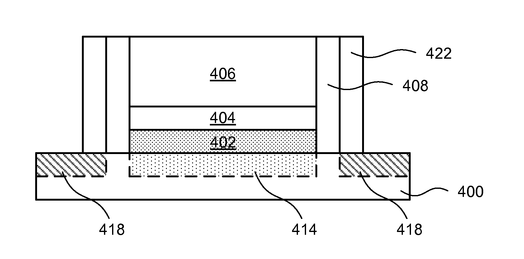
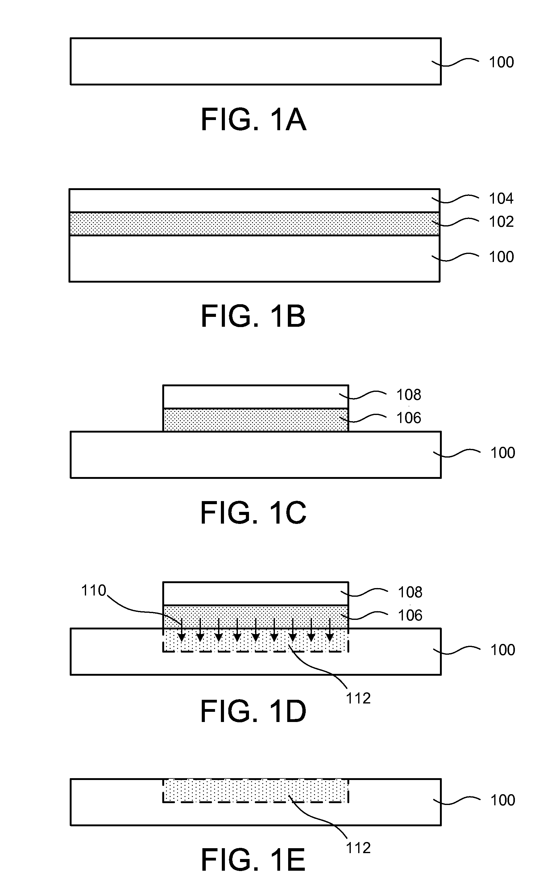
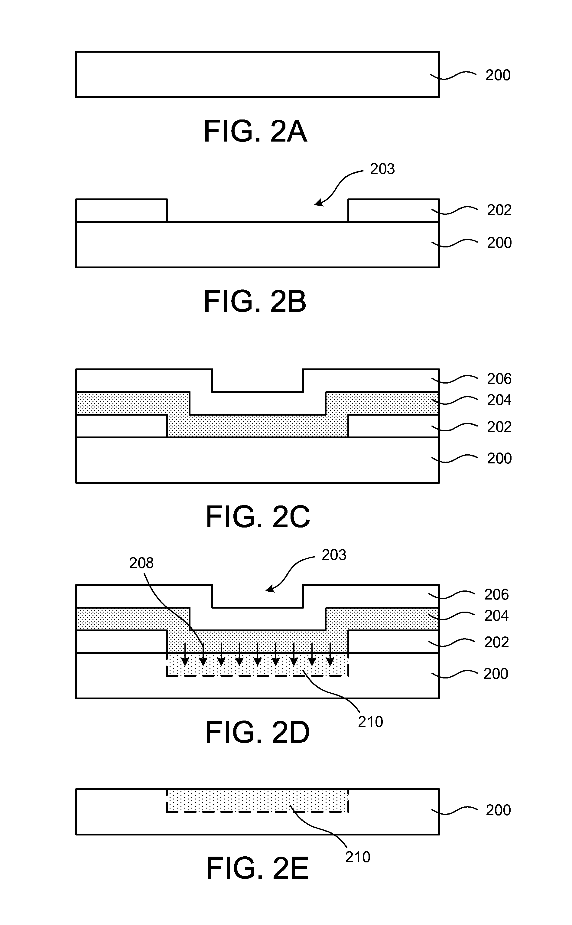
[0020]Methods for forming ultra-shallow dopant regions in semiconductor devices by solid phase diffusion from a dopant layer into a substrate layer are disclosed in various embodiments. The dopant regions can include, for example, ultra-shallow source-drain extensions for planar transistors, FinFETs, or tri-gate FETs. Other applications of ultra-shallow dopant region formation can include channel doping in replacement gate process flows, and for FinFET, or extremely thin silicon on insulator (ET-SOI) devices. Devices with extremely thin alternative semiconductor channels may also be doped using the disclosed method, for instance germanium on insulator devices (GeOI) or Ge FinFETs, and III-V channel devices such as GaAs, InGaAs, or InGaSb FinFETs. In addition, devices formed in amorphous Si or polycrystalline Si layers, such as EDRAM devices may utilize the disclosed method to adjust the Si doping level.

[0021]One skilled in the relevant art will recognize that the various embodiments...


PUM

PropertyMeasurementUnit
thicknessaaaaaaaaaa
sizeaaaaaaaaaa
sizeaaaaaaaaaa

Abstract

A method for forming an ultra-shallow boron dopant region in a substrate is provided. In one embodiment, the method includes depositing, by atomic layer deposition (ALD), a boron dopant layer in direct contact with the substrate, where the boron dopant layer contains an oxide, a nitride, or an oxynitride formed by alternating gaseous exposures of boron amide precursor or an organoboron precursor and a reactant gas. The method further includes patterning the dopant layer and forming an ultra-shallow dopant region in the substrate by diffusing boron from the boron dopant layer into the substrate by a thermal treatment.

Description

CROSS-REFERENCE TO RELATED APPLICATIONS[0001]This application is related to co-pending U.S. patent application Ser. No. ______ (Docket No. TTCA-373), entitled “METHOD FOR FORMING ULTRA-SHALLOW DOPING REGIONS BY SOLID PHASE DIFFUSION,” filed on even date herewith. The entire contents of this application are herein incorporated by reference in its entirety.FIELD OF INVENTION[0002]The present invention generally relates to semiconductor devices and methods for forming the same, and more particularly to ultra-shallow dopant region formation by solid phase diffusion from a dopant layer into a substrate layer.BACKGROUND OF THE INVENTION[0003]The semiconductor industry is characterized by a trend toward fabricating larger and more complex circuits on a given semiconductor chip. The larger and more complex circuits are achieved by reducing the size of individual devices within the circuits and spacing the devices closer together. As the dimensions of the individual components within a devic...

Claims


Application Information

Patent Timeline
Patent Type & Authority Applications(United States)
IPC IPC(8): H01L21/322
CPCH01L21/2254H01L21/2255H01L29/105H01L29/66545H01L29/6659H01L21/324H01L21/322H01L21/02175H01L21/0228H01L21/2256H01L21/31111H01L29/7391
Inventor CLARK, ROBERT D.
Owner TOKYO ELECTRON LTD
Why Eureka
Try Eureka