Light extraction substrate for electroluminescent device and manufacturing method thereof

a technology of electroluminescent devices and manufacturing methods, which is applied in the direction of solid-state devices, semiconductor devices, organic semiconductor devices, etc., can solve the problems of increasing cost, difficult to apply oleds to large-area illumination without an improvement in light extraction efficiency, and limited light extraction efficiency to about 30%, so as to increase the light extraction efficiency of the light extraction layer, high transparency, and high refractive index

Inactive Publication Date: 2012-10-18
SAMSUNG CORNING PRECISION MATERIALS CO LTD
View PDF5 Cites 32 Cited by
  • Summary
  • Abstract
  • Description
  • Claims
  • Application Information

AI Technical Summary

Benefits of technology

[0036]According to embodiments of the invention, it is possible to increase the light extraction efficiency of the light extraction layer by forming the light extraction layer from an inorganic oxide that has high transparency, a high refractive index, a strong force of bonding to the substrate, and a wide band gap.
[0037]In addition, according to embodiments of the i

Problems solved by technology

However, OLEDs in the stage of commercial distribution still have a problem in that light extraction efficiency is limited to about 30% because light loss occurs at the interface due to refractive index mismatching.
As a result, it is difficult to apply OLEDs to large area illumination without an improvement in the light extraction efficie

Method used


Image

  • Light extraction substrate for electroluminescent device and manufacturing method thereof
  • Light extraction substrate for electroluminescent device and manufacturing method thereof
  • Light extraction substrate for electroluminescent device and manufacturing method thereof

Examples


Embodiment Construction

[0043]Reference will now be made in detail to various embodiments of the present invention, examples of which are illustrated in the accompanying drawings and described below, so that a person having ordinary skill in the art to which the present invention relates can easily put the present invention into practice.

[0044]In the following description of the present invention, detailed descriptions of known functions and components incorporated herein will be omitted when they may make the subject matter of the present invention unclear.

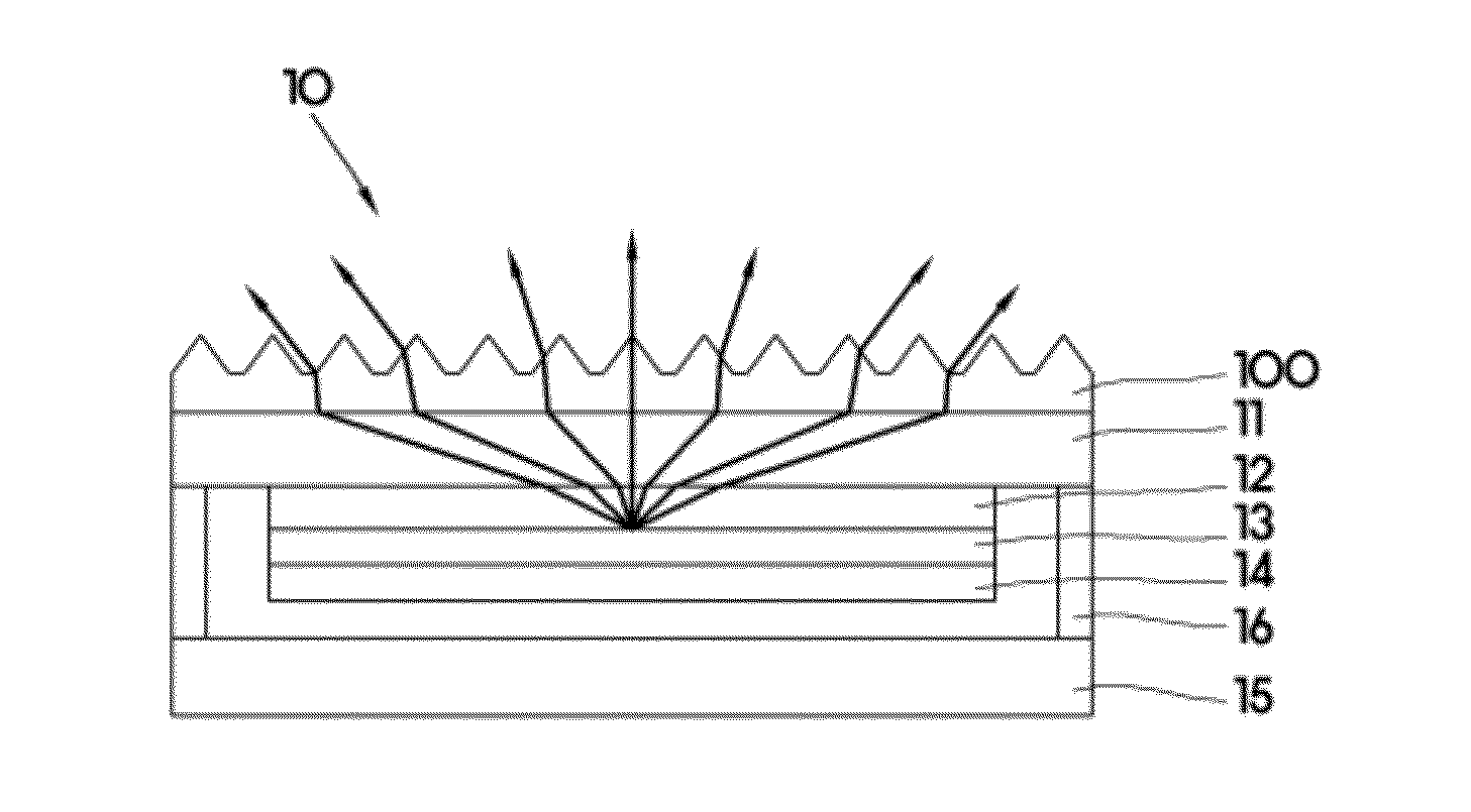
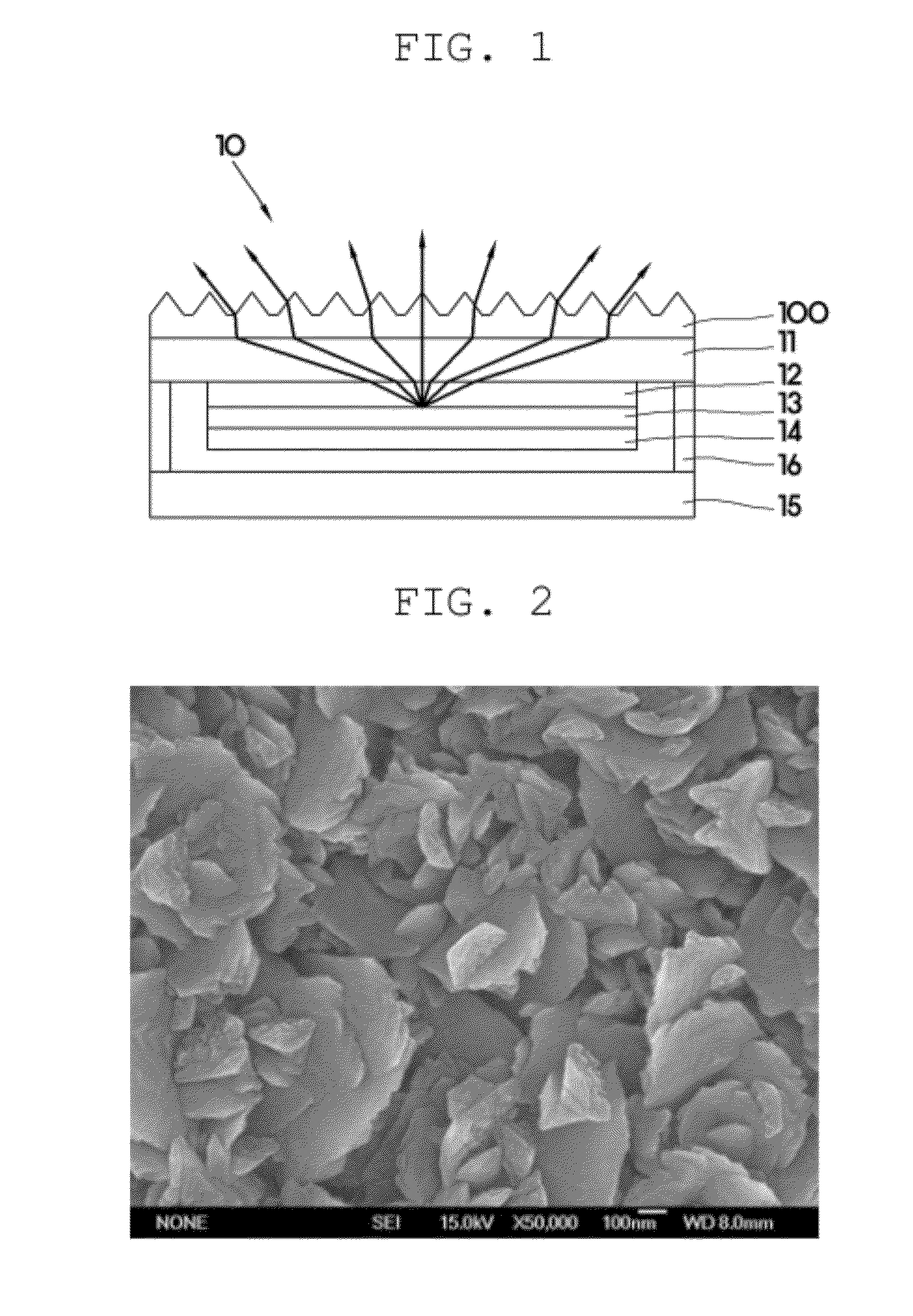
[0045]Referring to FIG. 1, a light extraction substrate for an organic light emitting diode (OLED) according to an embodiment of the invention includes a substrate 11 and a light extraction layer 100. The light extraction layer 100 is formed on the substrate 11. The light extraction layer 100 formed on the substrate 11 may have a thickness ranging from 30 nm to 4000 nm. In addition, the light extraction layer 100 may be implemented as an oxide thin film...


PUM


Abstract

A light extraction substrate for an electroluminescent device and a manufacturing method thereof, in which light extraction efficiency is increased. The light extraction substrate for an electroluminescent device includes a substrate and a light extraction layer formed on the substrate. The light extraction layer contains an oxide that has a wide band gap of 2.8 eV or more. The light extraction layer has a texture on the surface thereof.

Description

CROSS REFERENCE TO RELATED APPLICATION[0001]The present application claims priority from Korean Patent Application Numbers 10-2011-0035791 and 10-2011-0035792 filed on Apr. 18, 2011, the entire contents of which applications are incorporated herein for all purposes by this reference.BACKGROUND OF THE INVENTION[0002]1. Field of the Invention[0003]The present invention relates to a light extraction substrate for an electroluminescent device and a manufacturing method thereof, and more particularly, to a light extraction substrate for an electroluminescent device and a manufacturing method thereof, in which light extraction efficiency can be increased.[0004]2. Description of Related Art[0005]Electroluminescent devices are divided into inorganic electroluminescent devices and organic electroluminescent devices (OLEDs). Inorganic electroluminescent devices are represented by light-emitting diodes (LEDs).[0006]An OLED includes an anode, an organic luminescent layer, and a cathode, which a...

Claims


Application Information

Patent Timeline
IPC IPC(8): H01L51/50H01L33/60
CPCH01L33/22H01L2251/5369H01L51/5275H10K50/858H10K2102/331
Inventor YOO, YOUNGZOKIM, SEOHYUNPARK, JUNEHYOUNGPARK, TAEJUNGYOON, GUN SANGCHOI, EUN-HOPARK, JEONGWOO
Owner SAMSUNG CORNING PRECISION MATERIALS CO LTD
Why Eureka
Try Eureka