Soi device with dti and sti

Active Publication Date: 2012-10-18
GLOBALFOUNDRIES US INC
View PDF2 Cites 63 Cited by
  • Summary
  • Abstract
  • Description
  • Claims
  • Application Information

AI Technical Summary

Problems solved by technology

A challenge for enabling the back gat

Method used


Image

  • Soi device with dti and sti
  • Soi device with dti and sti
  • Soi device with dti and sti

Examples


Embodiment Construction

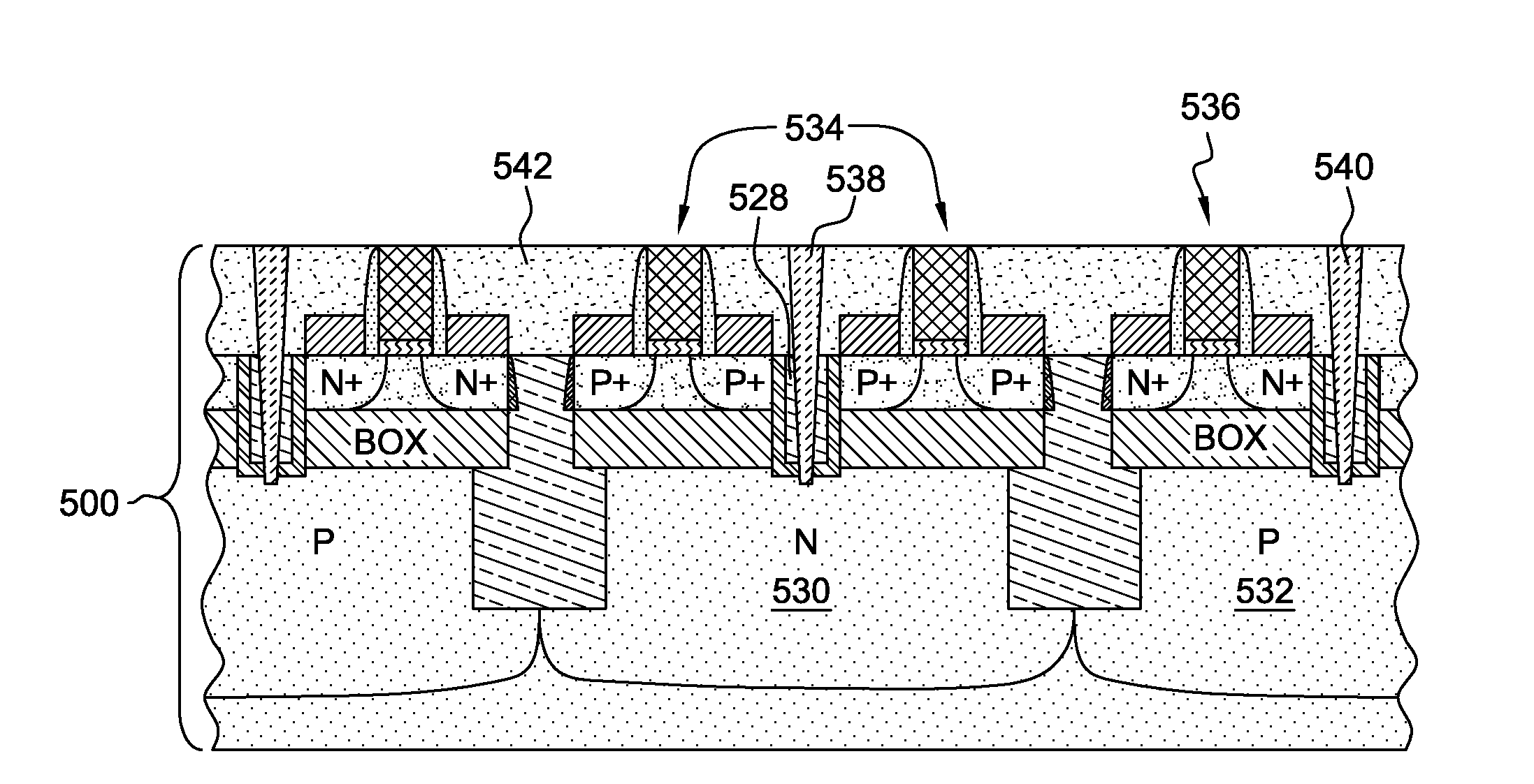
[0052]In order to tune the VT of N-type field effect transistor (NFET) and P-type field effect transistor (PFET) devices in ETSOI architecture, doping and / or back gate bias may be applied. Devices sharing the common back-gate bias may be isolated from the rest of the chip by deep-trench isolation. Within the deep-trench isolation region the individual devices may be separated from each other using shallow-trench isolation.

[0053]Accordingly, the present exemplary embodiments provide a structure and a method for forming an ETSOI circuit with a deep trench isolation for interwell (well to well) isolation and a shallow trench isolation for intrawell (within the same well) isolation. The lower portion of the deep trench isolation below the buried oxide layer may be enlarged to improve isolation and enhance process window, for example, to improve overlay tolerance.

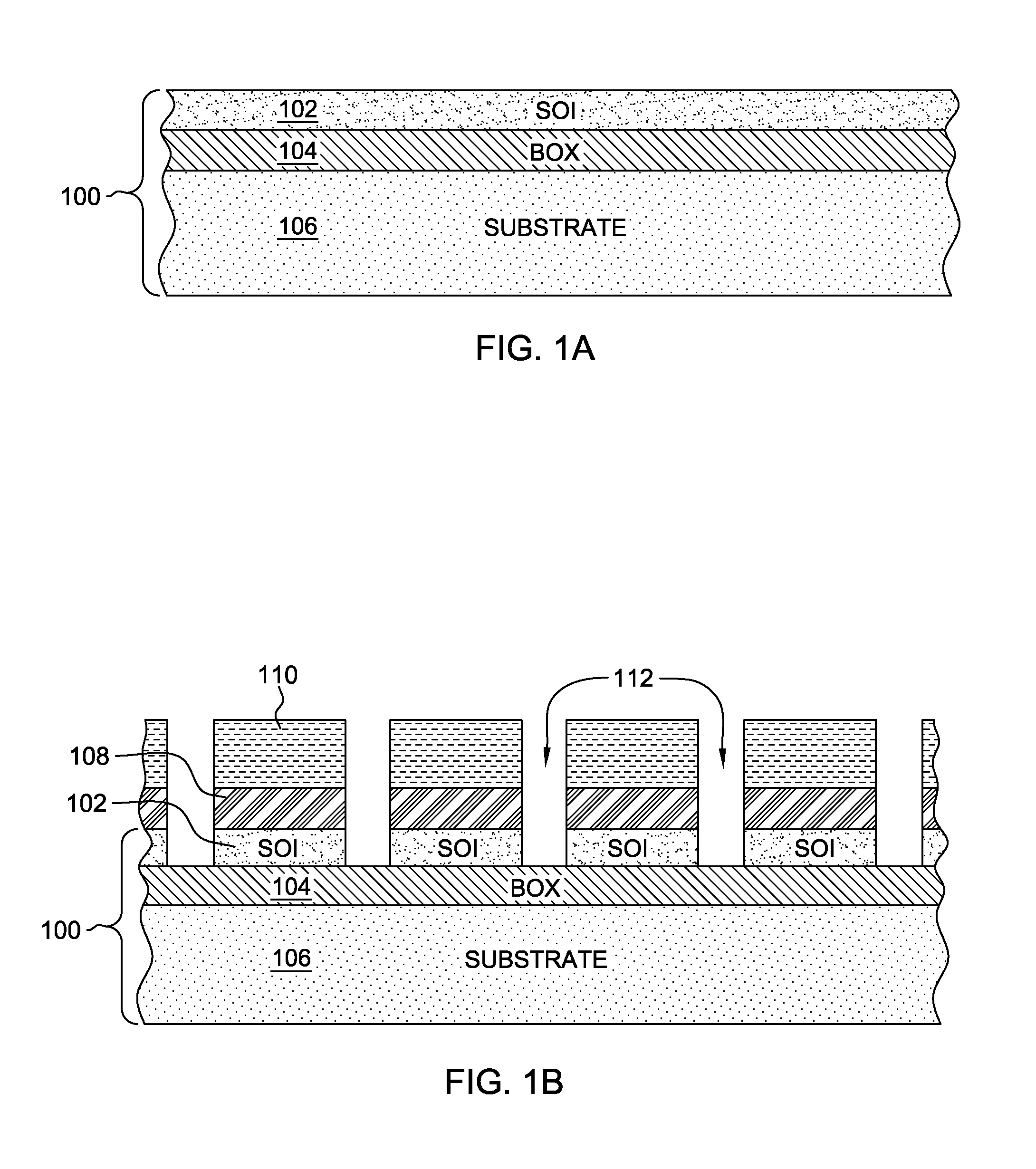
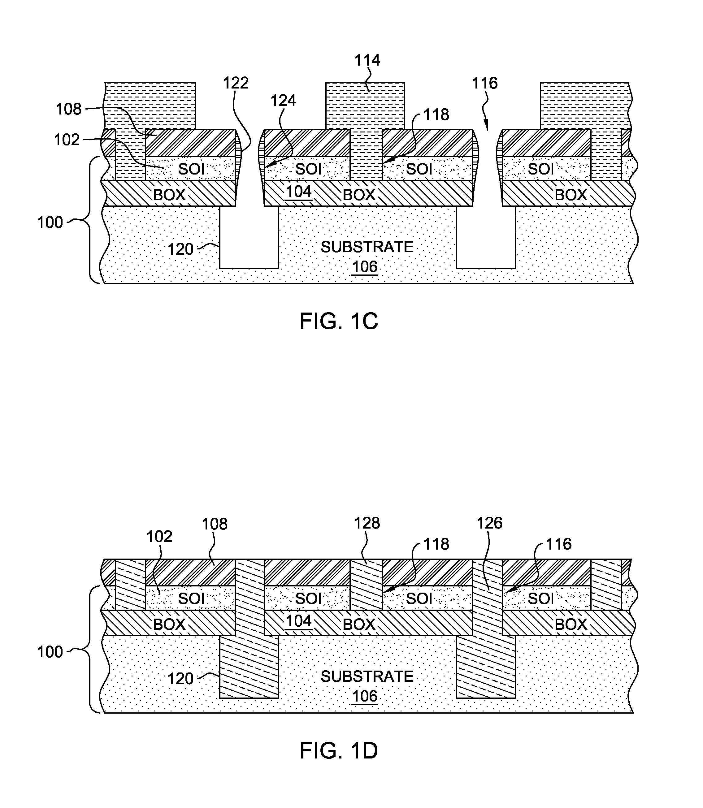
[0054]The present invention relates to the fabrication of a circuit on a semiconductor on insulator (SOI) substrate which incl...


PUM


Abstract

An SOI structure including a semiconductor on insulator (SOI) substrate including a top silicon layer, an intermediate buried oxide (BOX) layer and a bottom substrate; at least two wells in the bottom substrate; a deep trench isolation (DTI) separating the two wells, the DTI having a top portion extending through the BOX layer and top silicon layer and a bottom portion within the bottom substrate wherein the bottom portion has a width that is larger than a width of the top portion; and at least two semiconductor devices in the silicon layer located over one of the wells, the at least two semiconductor devices being separated by a shallow trench isolation within the top silicon layer.

Description

BACKGROUND[0001]The present invention relates to the fabrication of semiconductor devices on a semiconductor on insulator (SOI) substrate, and more particularly, to the fabrication of semiconductor devices on an extremely thin SOI substrate with improved isolation and a thin buried oxide layer.[0002]Extremely thin SOI substrates (ETSOI), also known as fully depleted SOI (FDSOI), rely on an ultra-thin semiconductor layer (for example, silicon) on a buried oxide layer. “Fully-depleted” means that the conducting channel of the transistor is depleted of charge by the time the transistor turns on which can only occur in SOI technologies because in bulk silicon there is an almost infinite source of charge available that cannot be depleted. The performance advantage of fully-depleted transistors comes from the fact that when there is no charge in the channel, the entire gate voltage is applied to create a conducting channel.[0003]ETSOI is a viable device option for extending CMOS scaling. ...

Claims


Application Information

Patent Timeline
IPC IPC(8): H01L27/12H01L21/76
CPCH01L21/84H01L27/1203H01L21/76229H01L21/76232H01L21/76283H01L21/743
Inventor CHENG, KANGGUODORIS, BRUCE B.KHAKIFIROOZ, ALIKULKARNI, PRANITA
Owner GLOBALFOUNDRIES US INC
Why Eureka
Try Eureka