

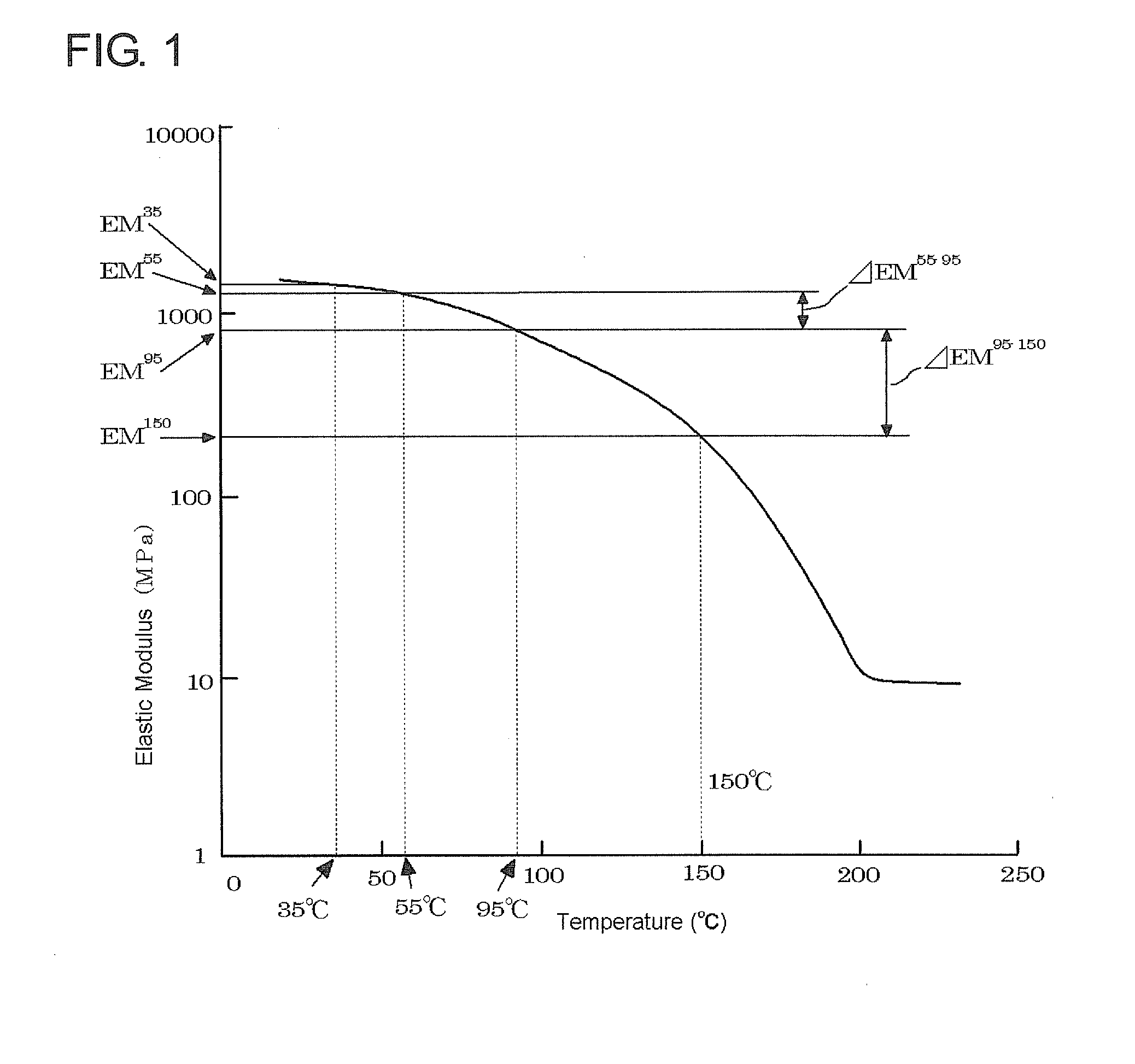
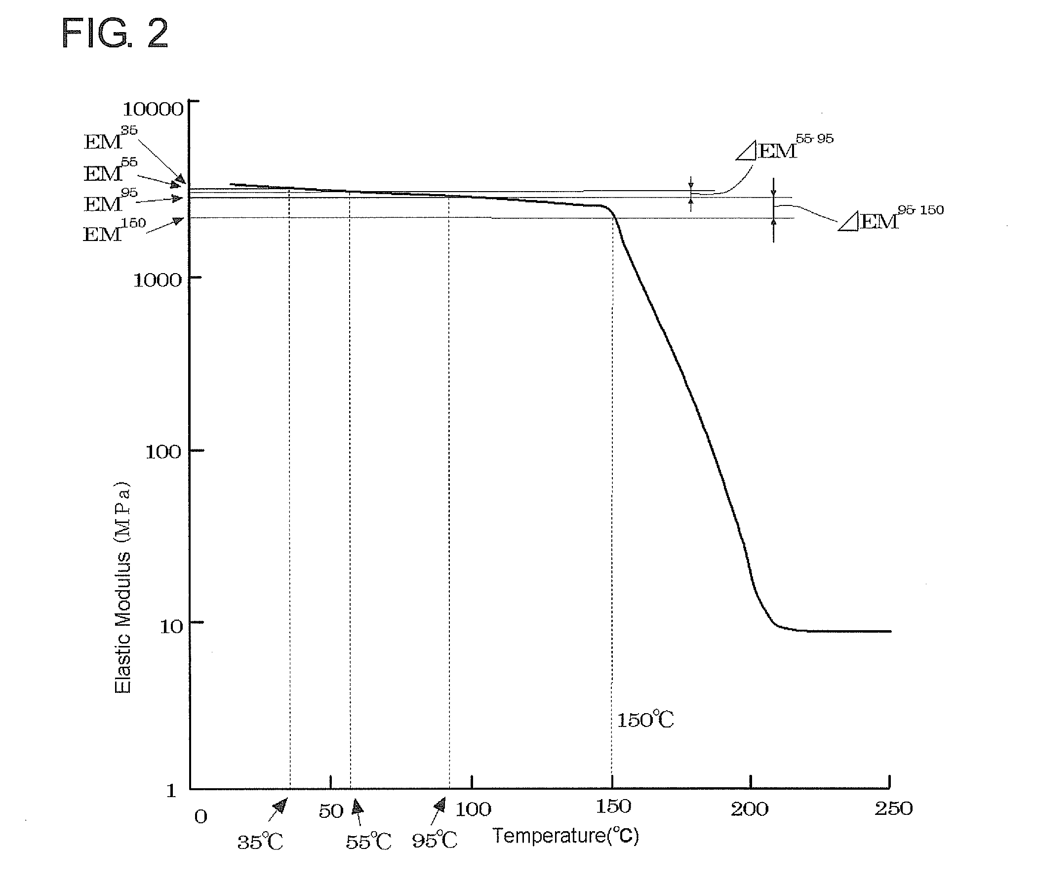
Anisotropic conductive adhesive
a conductive adhesive and anisotropic technology, applied in the direction of conductive materials, non-conductive materials with dispersed conductive materials, light support devices, etc., can solve the problems of significant reduction of conduction reliability, increase of conduction resistance between the chip and the circuit, and generation of internal stress due to the difference in thermal expansion coefficient between the circuit board and the chip. achieve the effect of high conduction reliability
- Summary
- Abstract
- Description
- Claims
- Application Information
AI Technical Summary
Benefits of technology
Problems solved by technology
Method used
Image

Examples
reference example 1
Production of Acrylic Resin A
[0035]A four-necked flask equipped with a stirrer and a condenser tube was charged with 100 g of ethyl acrylate (EA), 10 g of glycidyl methacrylate (GMA), 0.2 g of azobisbutyronitrile, 300 g of ethyl acetate, and 5 g of acetone. The mixture was subjected to a polymerization reaction at 70° C. for 8 hours under stirring. Then precipitated particles were collected by filtration, washed with ethanol, and dried to obtain acrylic resin A. The weight average molecular weight of the obtained acrylic resin A was 80,000, and its glass transition temperature was −40° C.
reference example 2
Production of Acrylic Resin B
[0036]A four-necked flask equipped with a stirrer and a condenser tube was charged with 100 g of ethyl acrylate (EA), 10 g of dimethylaminoethyl acrylate (DMAEA), 0.2 g of azobisbutyronitrile, 300 g of ethyl acetate, and 5 g of acetone. The mixture was subjected to a polymerization reaction at 70° C. for 8 hours under stirring. Then precipitated particles were collected by filtration, washed with ethanol, and dried to obtain acrylic resin B. The weight average molecular weight of the obtained acrylic resin B was 80,000, and its glass transition temperature was 18° C.
reference example 3
Production of Acrylic Resin C
[0037]A four-necked flask equipped with a stirrer and a condenser tube was charged with 100 g of butyl acrylate (BA), 10 g of glycidyl methacrylate (GMA), 0.2 g of azobisbutyronitrile, 300 g of ethyl acetate, and 5 g of acetone. The mixture was subjected to a polymerization reaction at 70° C. for 8 hours under stirring. Then precipitated particles were collected by filtration, washed with ethanol, and dried to obtain acrylic resin C. The weight average molecular weight of the obtained acrylic resin C was 80,000, and its glass transition temperature was −70° C.
PUM
| Property | Measurement | Unit |
|---|---|---|
| frequency | aaaaa | aaaaa |
| anisotropic conductive | aaaaa | aaaaa |
| elastic modulus | aaaaa | aaaaa |
Abstract
Description
Claims
Application Information