Active matrix device and method of driving the same

a technology of active matrix and device, applied in the field of digital microfluidics, can solve the problems of time required, low temperature change rate that can be achieved, and different droplets cannot have different temperatures within the same device at the same time, so as to simplify manufacturing and reduce costs

Active Publication Date: 2012-10-25
SHARP LIFE SCI EU LTD
View PDF1 Cites 35 Cited by
  • Summary
  • Abstract
  • Description
  • Claims
  • Application Information

AI Technical Summary

Benefits of technology

[0018]The heater capability can be implemented within the TFT control substrate thus simplifying manufacture and reducing cost

Problems solved by technology

This suffers from the disadvantages that the rates of temperature change that can be achieved are generally low, that a long time is required for the whole arrangement to reach thermal equilibrium.
Furthermore different droplets cannot simultaneously have different temperatures within the same device.
A disadvantage of this method is that the thermal resistance between the heat exchangers and the droplets will be relatively large since in general the substrates are fabricated from a poorly thermally conducting material, e.g. glass.
This will adversely affect the spatial resolution of the thermal control that can be achieved and also result in a long thermal time constant.
A disadvantage of U.S. Pat. No. 7,163,612 is that it does not disclose any circuit embodiments for realising the TFT backplane of the AM-EWOD.
A disadvantage of WO2010 / 041214 is that it does not describe any integrated means for moving the fluids between the different chambers of the device.

Method used


Image

  • Active matrix device and method of driving the same
  • Active matrix device and method of driving the same
  • Active matrix device and method of driving the same

Examples


first embodiment

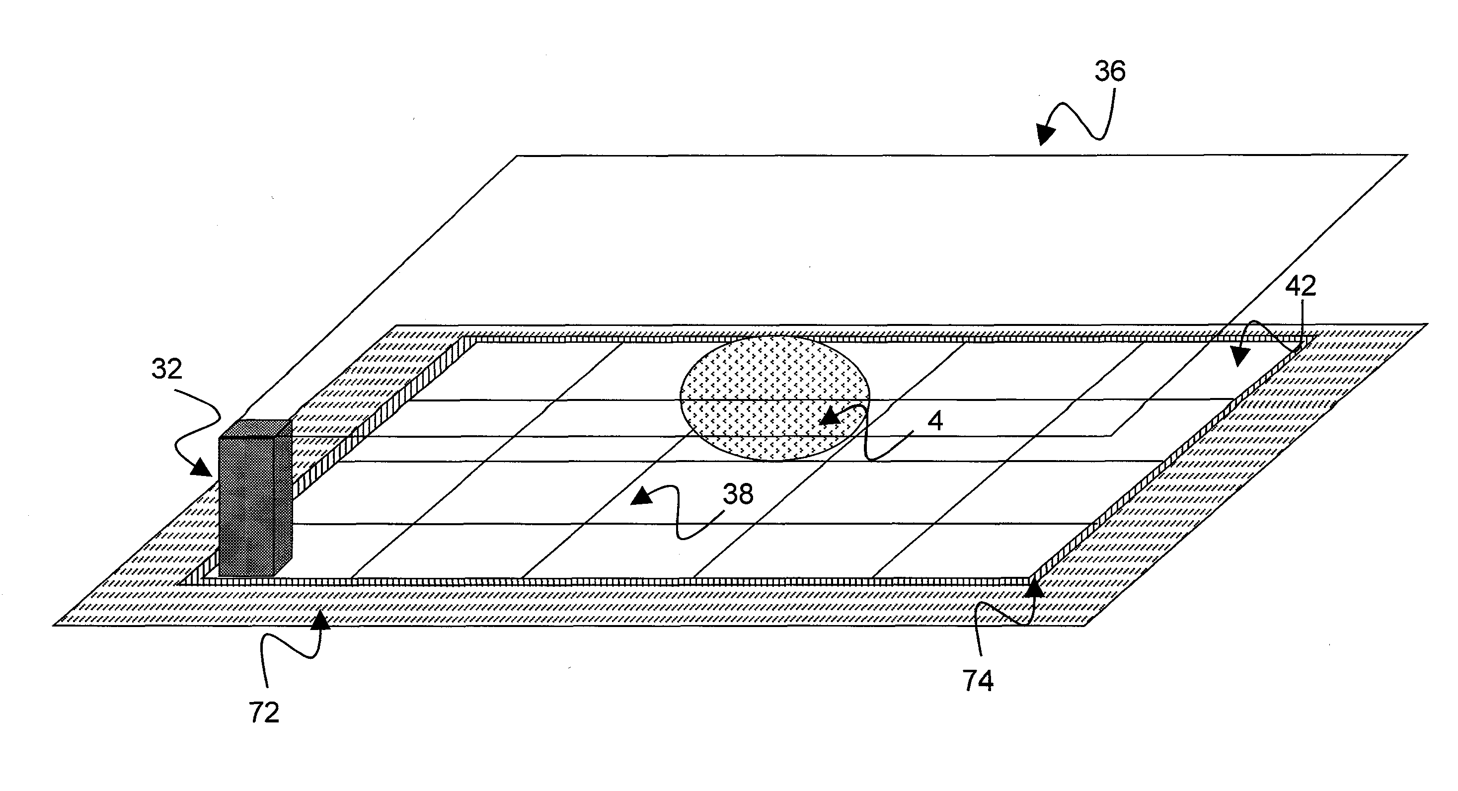
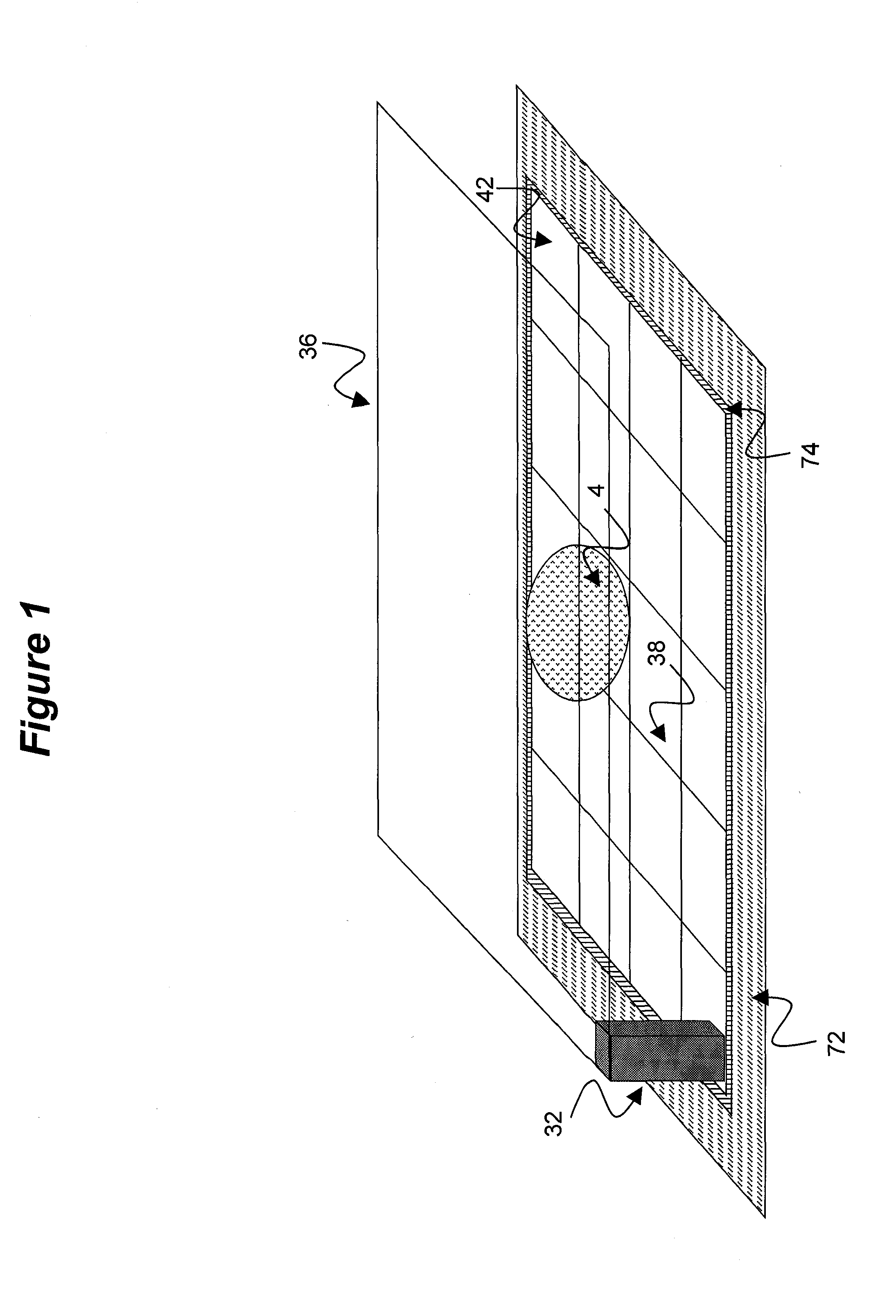
[0160]A second embodiment of the invention is as the first embodiment, where an alternative array element driver circuit for an array element 84 is used, shown FIG. 11.

[0161]The array element driver circuit according to this embodiment contains the following elements:[0162]A memory function 118 consisting of an SRAM cell and comprising:[0163]A column write line SL (originating from the column driver 78), which may be common to array elements within the same column[0164]A row select line GL (originating from the row driver 76), which may be common to array elements within the same row[0165]An n-type switch transistor 102[0166]A p-type switch transistor 104[0167]A first inverter 106[0168]A second inverter 108[0169]An inversion circuit 120 comprising:[0170]A first analog switch 114[0171]A second analog switch 116[0172]A voltage supply V1, which may be common to all elements within the array[0173]A second voltage V2, which may be common to all elements within the array

[0174]Heater array...

fourth embodiment

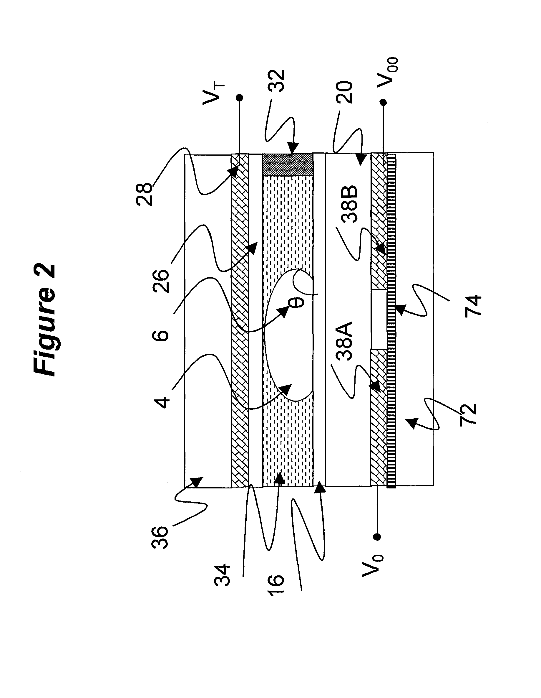
[0224]the invention is as any of the previous embodiments where the thin film electronics 74 additionally contains a temperature sensor element 130 as described in prior art. FIG. 18 shows a cross section of the device according to this embodiment. As shown in the figure, the temperature sensor element 130 may in some instances be arranged in close proximity to the second EW drive electrode 38D, for example where it is advantageous to get rapid feedback information from applied heating. In other instances it may be better to locate the temperature sensor further away from the second EW drive electrode 38D or to have a multipliplicty of temperature sensor elements 130 at different distances from the second EW drive electrode in order to determine the temperature profile at different locations within the device. One or more temperature sensor elements 130 may be included at the position of each standard array element 84 and / or heater array element to form an array of temperature senso...


PUM


Abstract

An electrowetting on dielectric (EWOD) device which includes a plurality of array elements configured to manipulate one or more droplets of fluid on an array, each of the array elements including a corresponding array element driver circuit, wherein each array element driver circuit includes: a top substrate electrode and a first drive electrode between which the one or more droplets may be positioned, the top substrate electrode being formed on a top substrate, and the first drive electrode being formed on a lower substrate; and circuitry configured to selectively provide drive voltages to the first drive electrode to move the one or more droplets among the plurality of array elements, and wherein at least one of the plurality of array elements includes: a heater element also formed on the lower substrate and configured to heat the one or more droplets when positioned between the top substrate electrode and the first drive electrode of the at least one array element; and circuitry configured to control the heater element.

Description

TECHNICAL FIELD[0001]The present invention relates to active matrix arrays and elements thereof.[0002]In a particular aspect, the present invention relates to digital microfluidics, and more specifically to active matrix electro-wetting-on-dielectric (AM-EWOD) devices. Electro-wetting-On-Dielectric (EWOD) is a known technique for manipulating droplets of fluid on an array. Active Matrix EWOD (AM-EWOD) refers to implementation of EWOD in an active matrix array, for example by using thin film transistors (TFTs). The invention further relates to methods of driving such devices.BACKGROUND ART[0003]Electro-wetting on dielectric (EWOD) is a well known technique for manipulating droplets of fluid by application of an electric field. It is thus a candidate technology for digital microfluidics for lab-on-a-chip technology. An introduction the basic principles of the technology” can be found in Digital microfluidics: is a true lab-on-a-chip possible?, R. B. Fair, Micofluid Nanofluid (2007) 3:...

Claims


Application Information

Patent Timeline
Patent Type & Authority Applications(United States)
IPC IPC(8): G02B26/00
CPCB01L3/502792B01L7/52G02B26/005B01L2400/0427B01L2200/147
Inventor HADWEN, BENJAMIN JAMES
Owner SHARP LIFE SCI EU LTD
Why Eureka
Try Eureka