Sublimation growth of sic single crystals

a single crystal, physical vapor technology, applied in the growth process of polycrystalline materials, crystal growth processes, carbides, etc., can solve the problems of excessive silicon- or carbon-containing vapors, volatile contaminants, harmful components, etc., and achieve the effect of negative effect on the growth process and crystal quality

Inactive Publication Date: 2012-11-15
II VI
View PDF5 Cites 28 Cited by
  • Summary
  • Abstract
  • Description
  • Claims
  • Application Information

AI Technical Summary

Benefits of technology

[0020]Venting the vapor into this chamber, however, has its problems. Specifically, the chamber or space surrounding the growth crucible is usually filled with thermal insulation made of purified, light-weight, fibrous graphite. The Si-containing vapor is very reactive toward graphite,...

Problems solved by technology

These harmful components include excessive silicon- o...

Method used


Image

  • Sublimation growth of sic single crystals
  • Sublimation growth of sic single crystals
  • Sublimation growth of sic single crystals

Examples


example 1

Growth of 3″ Diameter Semi-Insulating 6H SiC Crystal

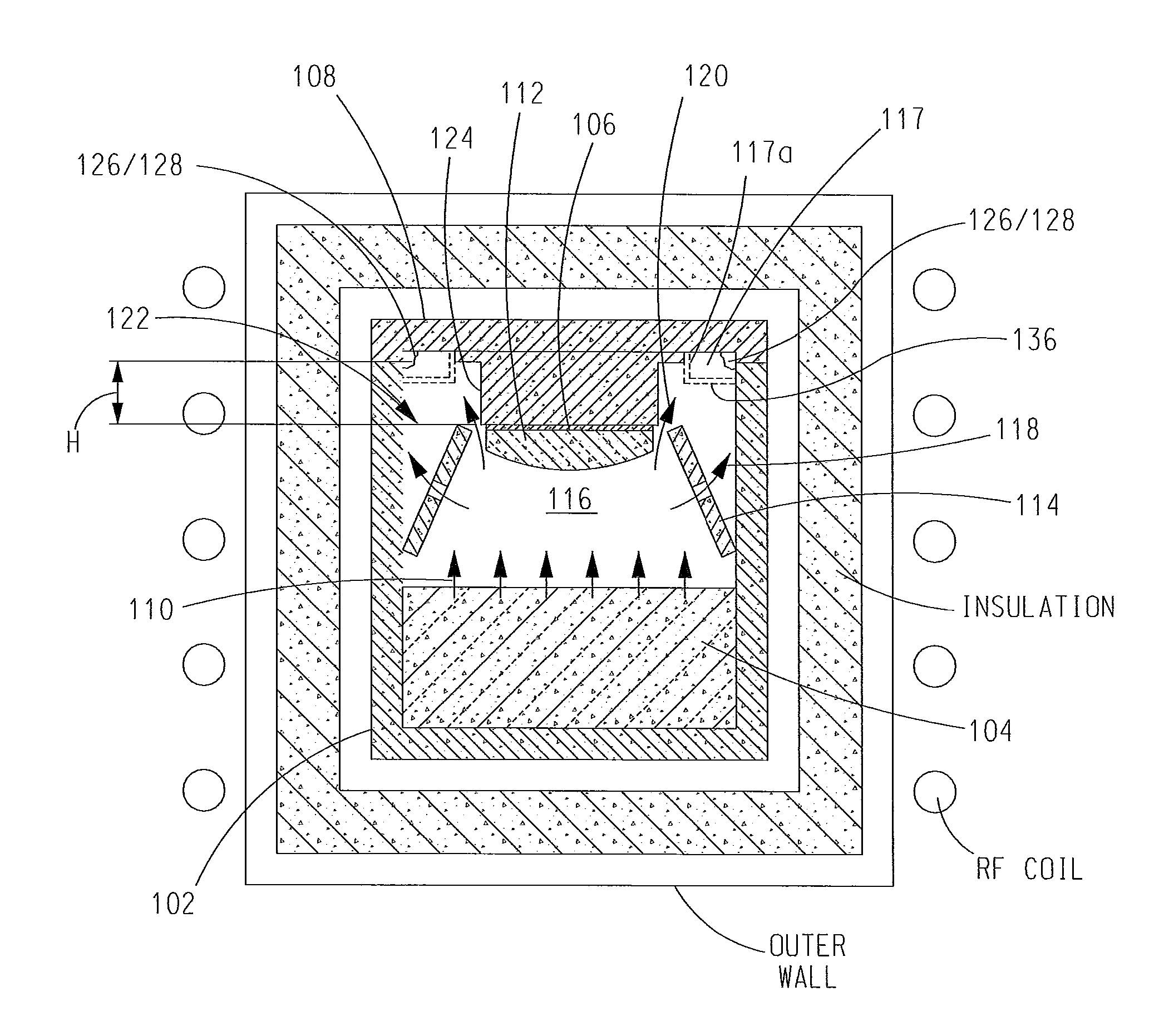
[0070]This growth run was carried out in a growth furnace having the crucible, baffle, and vapor-absorbing member 117a′ arrangement like the one shown in FIG. 6. In this growth run, a crystal growth crucible 102 made of dense, isostatically molded graphite was prepared and purified by high-temperature treatment in a halogen-containing atmosphere. High-purity SiC sublimation source material 104, i.e., SiC grains 0.5 to 2 mm in size, was synthesized prior to growth of SiC crystal 112 in a separate synthesis process. A charge of 600 g of the SiC source material 104 was disposed at the bottom of crucible 102 and served during growth of SiC crystal 112 as the solid sublimation source. In order to produce semi-insulating SiC crystal 112, the source material 104 included vanadium as a compensating dopant. The amount of vanadium and other details of vanadium doping were in accordance with the prior art.

[0071]A 3.25″ diameter SiC wafer of t...

example 2

Growth of 100 mm Diameter Semi-Insulating 6H SiC Crystal

[0077]This growth run gas was carried out in a growth furnace having the crucible, baffle, and vapor-absorbing member 117a″ arrangement like the one shown in FIG. 7. The crystal growth crucible 102 was made of dense, isostatically molded and halogen-purified graphite. High-purity SiC grain source material 104, 0.5 to 2 mm in size, was synthesized prior to growth in a separate synthesis process. A charge of 900 g of the SiC grain source material 104 was disposed at the bottom of crucible 102 and served during growth of SiC crystal 112 as a solid sublimation source.

[0078]A 110 mm diameter SiC wafer of the 6H polytype oriented on-axis was used as the seed crystal 106. The surface of the wafer where SiC crystal 112 was to grow was CMP polished prior to growth. The seed crystal 106 was attached to pedestal 124 of crucible lid 108 using a high-temperature adhesive. Pedestal 124 had a height of 10 mm.

[0079]Baffle 114″ used in this run...


PUM

PropertyMeasurementUnit
Temperatureaaaaaaaaaa
Fractionaaaaaaaaaa

Abstract

In SiC sublimation crystal growth, a crucible is charged with SiC source material and SiC seed crystal in spaced relation and a baffle is disposed in the growth crucible around the seed crystal. A first side of the baffle in the growth crucible defines a growth zone where a SiC single crystal grows on the SiC seed crystal. A second side of the baffle in the growth crucible defines a vapor-capture trap around the SiC seed crystal. The growth crucible is heated to a SiC growth temperature whereupon the SiC source material sublimates and forms a vapor which is transported to the growth zone where the SiC crystal grows by precipitation of the vapor on the SiC seed crystal. A fraction of this vapor enters the vapor-capture trap where it is removed from the growth zone during growth of the SiC crystal.

Description

BACKGROUND OF THE INVENTION[0001]1. Field of the Invention[0002]The present invention relates to Physical Vapor Transport growth of SiC single crystals.[0003]2. Description of Related Art[0004]Wafers of silicon carbide of the 4H and 6H polytype serve as lattice-matched substrates to grow epitaxial layers of SiC and GaN, which are used for fabrication of SiC- and GaN-based semiconductor devices for power and RF applications.[0005]Large, industrial-size SiC single crystals are grown by a sublimation technique commonly known as Physical Vapor Transport (PVT). PVT growth is usually carried out in a graphite crucible that includes solid SiC sublimation source material disposed, typically, at the crucible bottom and a SiC single crystal seed disposed, typically, at the crucible top. The sublimation source material is, usually, polycrystalline SiC grain synthesized separately. The loaded crucible is placed in a furnace and heated to the growth temperature, which is, generally, between 2000...

Claims


Application Information

Patent Timeline
IPC IPC(8): C30B23/02
CPCC01B31/36C30B29/36C30B23/005C01B32/956
Inventor GUPTA, AVINASH K.ZWIEBACK, ILYASEMENAS, EDWARDRENGARAJAN, VARATHARAJANGETKIN, MARCUS L.
Owner II VI
Why Eureka
Try Eureka