Photovoltaic cell, including a crystalline silicon oxide passivation thin film, and method for producing same

a photovoltaic cell and crystalline silicon oxide technology, applied in photovoltaic energy generation, electrical equipment, climate sustainability, etc., can solve the problems of not being able to smooth the sides of the pyramids and not being able to achieve the smooth side of the pyramid on the nanometric level. achieve good surface passivation and be easy to implemen

Active Publication Date: 2012-11-22
COMMISSARIAT A LENERGIE ATOMIQUE ET AUX ENERGIES ALTERNATIVES
View PDF9 Cites 14 Cited by
  • Summary
  • Abstract
  • Description
  • Claims
  • Application Information

AI Technical Summary

Benefits of technology

[0019]The object of the invention is to propose a heterojunction photovoltaic cell with a good surface passivation, while being easy to implement.

Problems solved by technology

However, the step of texturing at least one face of the substrate, almost always necessary, does not facilitate the good uniform distribution of these layers.
However, the sides of the obtained pyramids are often very rough and the summits and valleys of the pyramids are abrupt (radius of curvature in general lower than 30 nm), which is detrimental to a perfect thickness uniformity for the layers successively deposited on the textured face.
However, this etching is too important, about 2 μm or more, and it does not make it possible to smooth the sides of the pyramids on the nanometric level.
In addition, the texturing step, as well as the cleaning steps, the etching steps and the waiting times before the depositions can generate a (particulate and / or metal) contamination of the surface of the textured face of the substrate, which causes an important increase of the state density of the surface of the textured substrate.
Thus, these problems of pollution are detrimental to a good passivation of the surface and thus to high outputs despite the use of a transition layer of intrinsic amorphous silicon as a passivation layer.
However, making such a passivation layer causes the formation of many defects at the interface between the n-doped crystalline silicon substrate and said passivation layer.

Method used


Image

  • Photovoltaic cell, including a crystalline silicon oxide passivation thin film, and method for producing same
  • Photovoltaic cell, including a crystalline silicon oxide passivation thin film, and method for producing same
  • Photovoltaic cell, including a crystalline silicon oxide passivation thin film, and method for producing same

Examples


Embodiment Construction

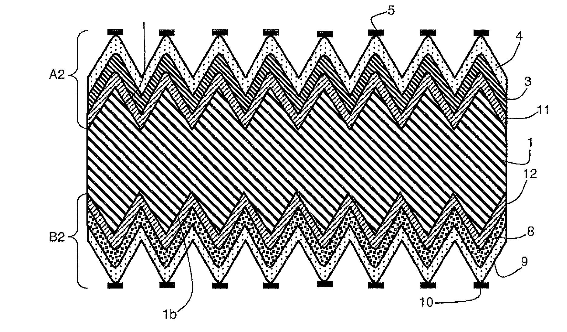
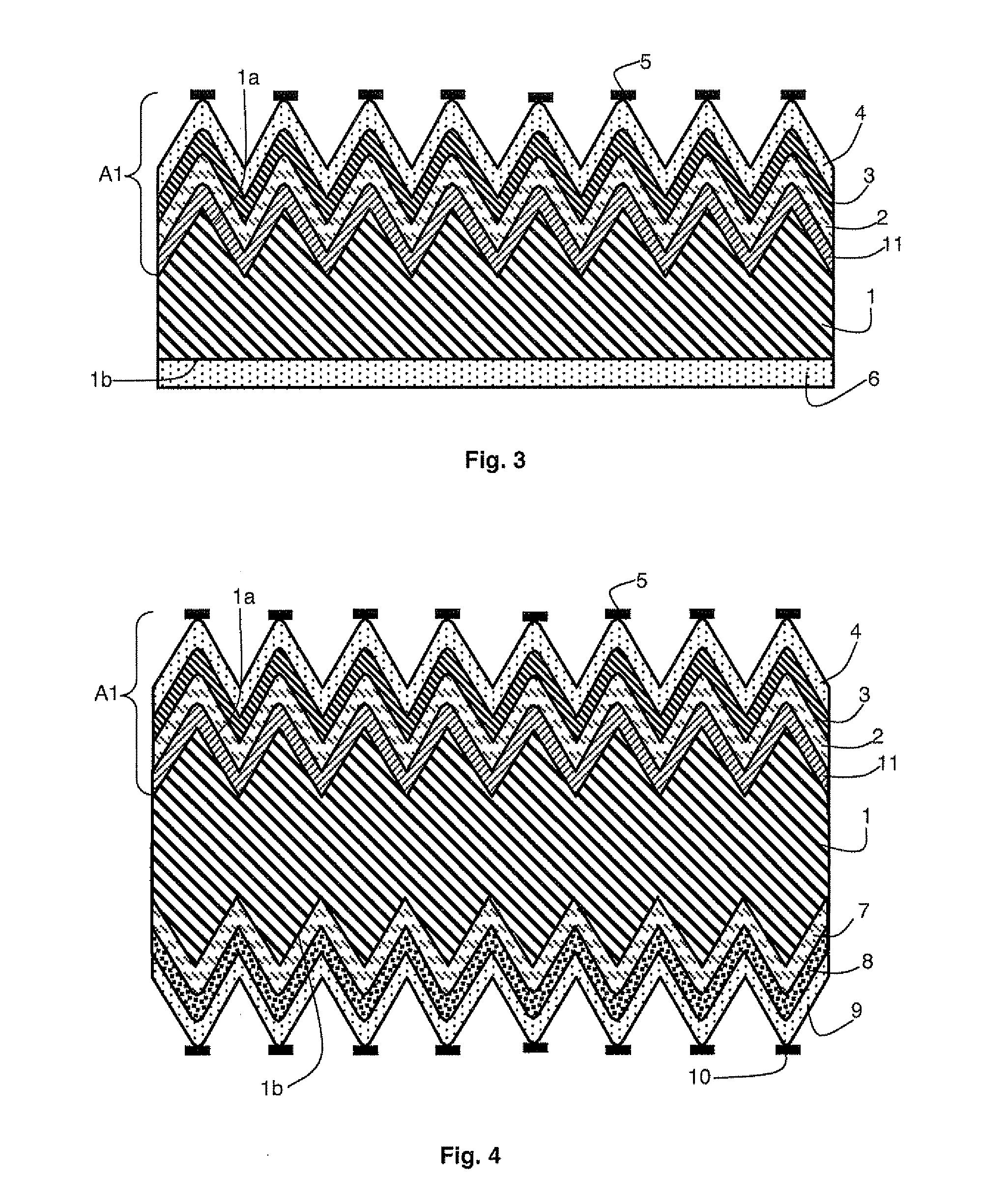
[0028]The photovoltaic cell according to FIG. 3 has a multi-layer stack substantially similar to that of the photovoltaic cell represented in FIG. 1. However, in FIG. 3, a crystalline silicon oxide thin film 11 is deposited between the crystalline silicon substrate 1 and the thin layer of intrinsic amorphous silicon 2.

[0029]The unit formed by the thin film 11, the layer of intrinsic amorphous silicon 2, the layer of p-doped amorphous silicon 3, the electrode 4 and the current collector 5 then constitute a multi-layer stack arranged on the front face 1a of the substrate 1 and noted A1 in FIG. 3.

[0030]More particularly, the thin film 11 is arranged directly on the front face 1a of the substrate 1 of n-doped crystalline silicon, between said substrate 1 and the layer 2 of intrinsic amorphous silicon. Consequently, it is directly in contact with the front face 1a of the substrate 1. Moreover, advantageously, it has a thickness lower than or equal to 2 nanometers and still advantageously...


PUM


Abstract

A heterojunction photovoltaic cell includes at least one crystalline silicon oxide film directly placed onto one of the front or rear faces of a crystalline silicon substrate, between said substrate and a layer of amorphous or microcrystalline silicon. The thin film is intended to enable the passivation of said face of the substrate. The thin film is more particularly obtained by radically oxidizing a surface portion of the substrate, before depositing the layer of amorphous silicon. Moreover, a thin layer of intrinsic or microdoped amorphous silicon can be placed between said think film and the layer of amorphous or microcrystalline silicon.

Description

TECHNICAL FIELD OF THE INVENTION[0001]The invention relates to a heterojunction photovoltaic cell including a crystalline silicon substrate with a given doping type and a layer of amorphous or microcrystalline silicon, as well as a method for producing at least one such a photovoltaic cell.STATE OF THE ART[0002]A heterojunction photovoltaic cell is made of a multi-layer stack making it possible to directly convert the photons received into an electric signal. The heterojunction is in particular formed by a crystalline silicon substrate of a given doping type (n or p) and by an amorphous silicon layer of a doping type opposite to that of the substrate.[0003]Moreover, an intermediate layer, called “electric passivation” layer, is generally placed between the two elements forming the heterojunction, in order to improve the interface characteristics of the heterojunction and thus the effectiveness of the conversion. As indicated in the patent application US2001 / 0029978, this intermediat...

Claims


Application Information

Patent Timeline
IPC IPC(8): H01L31/077H01L31/0352H01L31/18H01L31/075H01L31/0745H01L31/0747
CPCH01L31/0745H01L31/0747Y02E10/50H01L31/1868Y02E10/547Y02E10/548Y02P70/50H01L31/0368H01L31/03762
Inventor MUR, PIERREMORICEAU, HUBERTRIBEYRON, PIERRE-JEAN
Owner COMMISSARIAT A LENERGIE ATOMIQUE ET AUX ENERGIES ALTERNATIVES
Why Eureka
Try Eureka