
Line-tunneling tunnel field-effect transistor (TFET) and manufacturing method

a field-effect transistor and tunnel tunnel technology, applied in the field of line-tunnel tunnel field-effect transistors and manufacturing methods, can solve the problems of low on-current of all-silicon tfets, difficult to reduce supply voltage, and increase power consumption

Inactive Publication Date: 2012-11-29
INTERUNIVERSITAIR MICRO ELECTRONICS CENT (IMEC VZW) +2
View PDF0 Cites 32 Cited by
  • Summary
  • Abstract
  • Description
  • Claims
  • Application Information

AI Technical Summary

Benefits of technology

[0064]It is an advantage of the present invention that the spread of the onset voltage Vonset (i.e., the gate voltage at which BTBT tunneling occurs) with variations in the source-drain voltage VDS can be reduced significantly especially for semiconductor devices According to certain embodiments with small gate dielectric thickness (i.e., smaller equivalent oxide thickness EOT).
[0065]For purposes of summarizing the invention and the advantages achieved over the prior art, certain objects and advantages of the invention have been described herein above. Of course, it is to be understood that not necessarily all such objects or advantages may be achieved in accordance with any particular embodiment of the invention. Thus, for example, those skilled in the art will recognize that the invention may be embodied or carried out in a manner that achieves or optimizes one advantage or group of advantages as taught herein without necessarily achieving other objects or advantages as may be taught or suggested herein.
[0066]The above and other aspects of the invention will be apparent from and elucidated with reference to the embodiment(s) described hereinafter.

Problems solved by technology

One of the problems due to the scaling down of CMOS transistors is that the power consumption keeps increasing.
This is partly because leakage currents are increasing (e.g., due to short channel effects) and because it becomes difficult to decrease the supply voltage.
However, all-silicon TFETs typically suffer from low on-currents, a drawback related to the large resistance of the tunnel barrier.

Method used


Image

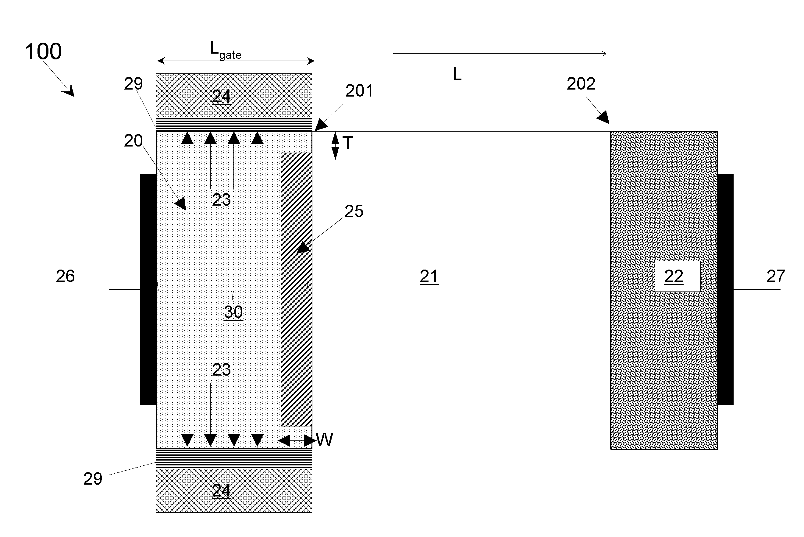
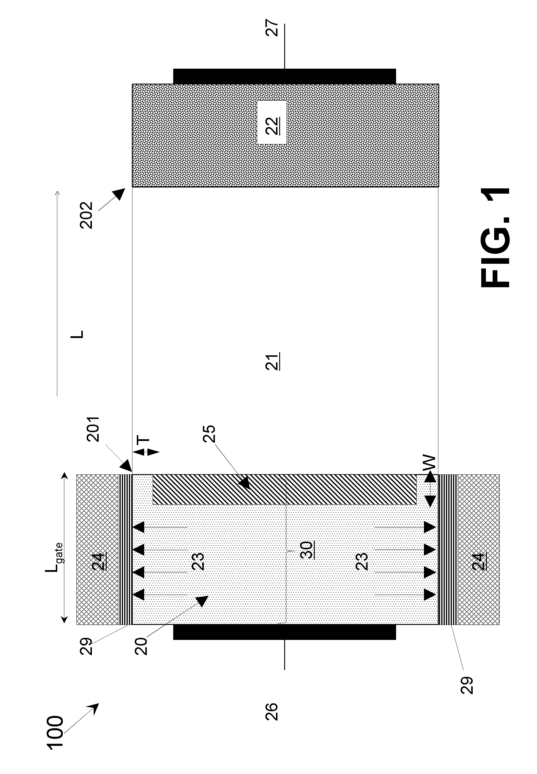
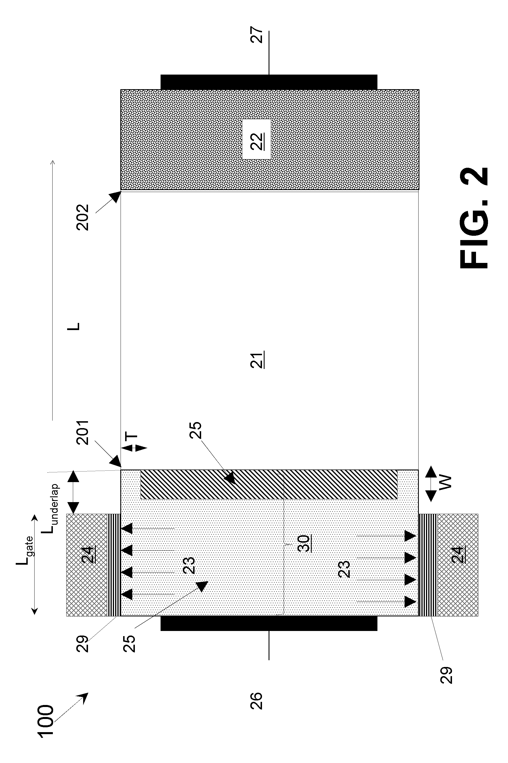
  • Line-tunneling tunnel field-effect transistor (TFET) and manufacturing method
  • Line-tunneling tunnel field-effect transistor (TFET) and manufacturing method
  • Line-tunneling tunnel field-effect transistor (TFET) and manufacturing method

Examples


Embodiment Construction

[0077]The present invention will be described with respect to particular embodiments and with reference to certain drawings but the invention is not limited thereto but only by the claims. The drawings described are only schematic and are non-limiting. In the drawings, the size of some of the elements may be exaggerated and not drawn on scale for illustrative purposes. The dimensions and the relative dimensions do not correspond to actual reductions to practice of the invention.

[0078]Moreover, the term top and the like in the description and the claims are used for descriptive purposes and not necessarily for describing relative positions. It is to be understood that the terms so used are interchangeable under appropriate circumstances and that the particular embodiments described herein are capable of operation in other orientations than described or illustrated herein.

[0079]It is to be noticed that the term “comprising”, used in the claims, should not be interpreted as being restr...


PUM


Abstract

A tunnel field effect transistor (TFET) and method of making the same is provided. The TFET comprises a source-channel-drain structure and a gat electrode. The source region comprises a first source sub-region which is doped with a first doping profile with a dopant element of a first doping type having a first peak concentration and a second source sub-region close to a source-channel interface which is doped with a second doping profile with a second dopant element with the same doping type as the first dopant element and having a second peak concentration. The second peak concentration of the second doping profile is substantially higher than the maximum doping level of the first doping profile close to an interface between the first and the second source sub-regions.

Description

CROSS-REFERENCE TO RELATED APPLICATIONS[0001]This application claims the benefit under 35 U.S.C. §119(e) of U.S. provisional application Ser. No. 61 / 488,934, filed May 23, 2011, and claims the benefit under 35 U.S.C. §119(a)-(d) of European application No. 11173950.4, filed Jun. 14, 2011, the disclosures of which are hereby expressly incorporated by reference in their entirety and are hereby expressly made a portion of this application.FIELD OF THE INVENTION[0002]The embodiments relate to the field of semiconductor devices and nanotechnology. More specifically, the embodiments relate to tunnel field effect transistors (TFET) where the tunnelling effect is based on band-to-band tunnelling. Furthermore the embodiments relate to a method for manufacturing a semiconductor device, more particularly to a method for fabricating tunnel field effect transistors. More specifically the fabrication method relates to but is not limited to standard planar technology, double gate technology, FINFE...

Claims


Application Information

Patent Timeline
IPC IPC(8): H01L29/775H01L21/20B82Y40/00
CPCB82Y10/00H01L29/7391H01L29/0665
Inventor VERHULST, ANNE S.KAO, KUO-HSING
Owner INTERUNIVERSITAIR MICRO ELECTRONICS CENT (IMEC VZW)
Learn More